Renesas Sets New MCU Performance Bar with 1-GHz RA8P1 Devices with AI Acceleration

发布时间:2025-07-04 14:56
作者:AMEYA360
来源:Renesas
阅读量:210
  • Unprecedented 7300+ CoreMarks1 with Dual Arm CPU cores

  • TSMC 22ULL Process Delivers High Performance and Low Power Consumption

  • Embedded MRAM with Faster Write Speeds and Higher Endurance and Retention

  • Dedicated Peripherals Optimized for Vision and Voice AI plus Real-Time Analytics

  • New AI Software Framework Eases Development and Enables Easy Migration with MPUs

  • Leading-Edge Security Features Ensure Data Privacy

  Renesas Electronics Corporation (TSE:6723), a premier supplier of advanced semiconductor solutions, introduced the RA8P1 microcontroller (MCU) Group targeted at Artificial Intelligence (AI) and Machine Learning (ML) applications, as well as real-time analytics. The new MCUs establish a new performance level for MCUs by combining 1GHz Arm® Cortex®-M85 and 250MHz Cortex-M33 CPU cores with the Arm Ethos™-U55 Neural Processing Unit (NPU). This combination delivers the highest CPU performance of over 7300 CoreMarks and AI performance of 256 GOPS at 500 MHz.
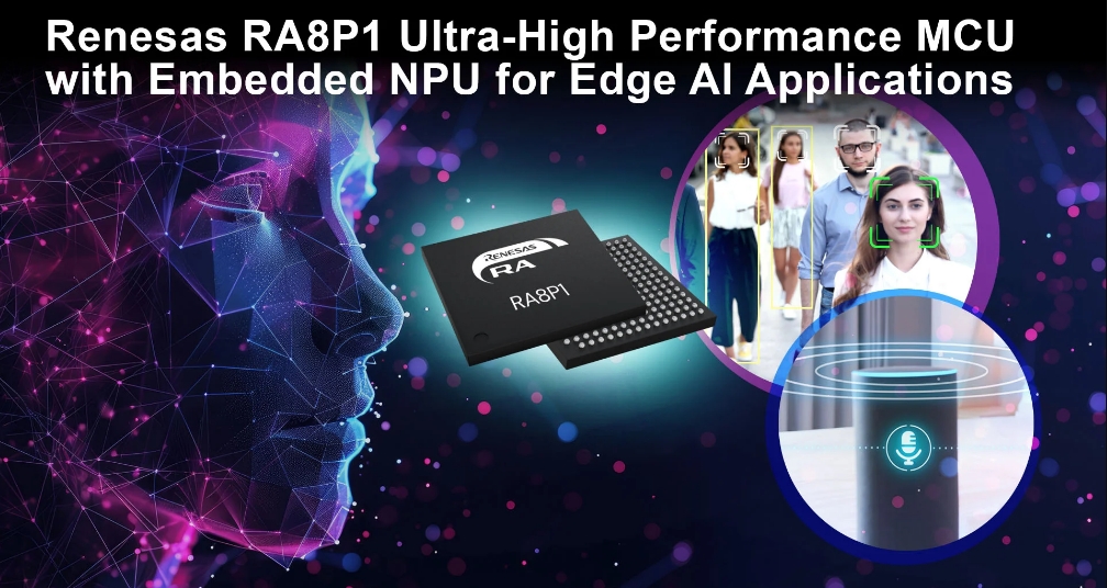
Renesas Sets New MCU Performance Bar with 1-GHz RA8P1 Devices with AI Acceleration

  Designed for Edge/Endpoint AI

  The RA8P1 is optimized for edge and endpoint AI applications, using the Ethos-U55 NPU to offload the CPU for compute intensive operations in Convolutional and Recurrent Neural Networks (CNNs and RNNs) to deliver up to 256 MACs per cycle that yield 256 GOPS performance at 500 MHz. The new NPU supports most commonly used networks, including DS-CNN, ResNet, Mobilenet TinyYolo and more. Depending on the neural network used, the Ethos-U55 provides up to 35x more inferences per second than the Cortex-M85 processor on its own.

  Advanced Technology

  The RA8P1 MCUs are manufactured on the 22ULL (22nm ultra-low leakage) process from TSMC, enabling ultra-high performance with very low power consumption. This process also enables the use of embedded Magnetoresistive RAM (MRAM) in the new MCUs. MRAM offers faster write speeds along with higher endurance and retention compared with Flash.

  “There is explosive growth in demand for high-performance edge AIoT applications. We are thrilled to introduce what we believe are the best MCUs to address this trend,” said Daryl Khoo, Vice President of Embedded Processing Marketing Division at Renesas. “The RA8P1 devices showcase our technology and market expertise and highlight the strong partnerships we have built across the industry. Customers are eager to employ these new MCUs in multiple AI applications.”

  “The pace of innovation in the age of AI is faster than ever, and new edge use cases demand ever-improving performance and machine learning on-device,” said Paul Williamson, Senior Vice President and General Manager, IoT Line of Business at Arm. “By building on the advanced AI capabilities of the Arm compute platform, Renesas’ RA8P1 MCUs meet the demands of next generation voice and vision applications, helping to scale intelligent, context-aware AI experiences.”

  “It is gratifying to see Renesas harness the performance and reliability of TSMC 22ULL embedded MRAM technology to deliver outstanding results for its RA8P1 devices,” said Chien-Hsin Lee, Senior Director of Specialty Technology Business Development at TSMC. “As TSMC continues to advance our embedded non-volatile memory (eNVM) technologies, we look forward to strengthening our long-standing collaboration with Renesas to drive innovation in future groundbreaking devices.”

  Robust, Optimized Peripheral Set for AI

  Renesas has integrated dedicated peripherals, ample memory and advanced security to address Voice and Vision AI and Real-time Analytics applications. For vision AI, a 16-bit camera interface (CEU) is included that supports sensors up to 5 megapixels, enabling camera and demanding Vision AI applications. A separate MIPI CSI-2 interface offers a low pin-count interface with two lanes, each up to 720Mbps. In addition, multiple audio interfaces including I2S and PDM support microphone inputs for voice AI applications.

  The RA8P1 offers both on-chip and external memory options for efficient, low latency neural network processing. The MCU includes 2MB SRAM for storing intermediate activations or graphics framebuffers. 1MB of on-chip MRAM is also available for application code and storage of model weights or graphics assets. High-speed external memory interfaces are available for larger models. SIP options with 4 or 8 MB of external flash in a single package are also available for more demanding AI applications.

  New RUHMI Framework

  Along with the RA8P1 MCUs, Renesas has introduced RUHMI (Renesas Unified Heterogenous Model Integration), a comprehensive framework for MCUs and MPUs. RUHMI offers efficient AI deployment of the latest neural network models in a framework agnostic manner. It enables model optimization, quantization, graph compilation and conversion, and generates efficient source code. RUHMI provides native support for machine-learning AI frameworks such as TensorFlow Lite, Pytorch & ONNX. It also provides the necessary tools, APIs, code-generator, and runtime needed to deploy a pre-trained neural network, including ready-to-use application examples and models optimized for RA8P1. RUHMI is integrated with Renesas’s own e2Studio IDE to allow seamless AI development. This integration will facilitate a common development platform for MCUs and MPUs.

  Advanced Security Features

  The RA8P1 MCUs provide leading-edge security for critical applications. The new Renesas Security IP (RSIP-E50D) includes numerous cryptographic accelerators, including CHACHA20, Ed25519, NIST ECC curves up to 521 bits, enhanced RSA up to 4K, SHA2 and SHA3. In concert with Arm TrustZone®, this provides a comprehensive and fully integrated secure element-like functionality. The new MCUs also provides strong hardware Root-of-Trust and Secure Boot with First Stage Bootloader (FSBL) in immutable storage. XSPI interfaces with decryption-on-the-fly (DOTF) allow encrypted code images to be stored in external flash and decrypted on the fly as it is securely transferred to the MCU for execution.

  Ready to Use Solutions

  Renesas provides a wide range of easy-to-use tools and solutions for the RA8P1 MCUs, including the Flexible Software Package (FSP), evaluation kits and development tools. FreeRTOS and Azure RTOS are supported, as is Zephyr. Several Renesas software example projects and application notes are available to enable faster time to market. In addition, numerous partner solutions are available to support development with the RA8P1 MCUs, including a driver monitoring solution from Nota.AI and a traffic/pedestrian monitoring solution from Irida Labs. Other solutions can be found at the Renesas RA Partner Ecosystem Solutions Page.

  Key Features of the RA8P1 MCUs

  Processors: 1GHz Arm Cortex-M85, 500MHz Ethos-U55, 250 MHz Arm Cortex-M33 (Optional)

  Memory: 1MB/512KB On-chip MRAM, 4MB/8MB External Flash SIP Options, 2MB SRAM fully ECC protected, 32KB I/D caches per core

  Graphics Peripherals: Graphics LCD controller supporting resolutions up to WXGA (1280x800), parallel RGB and MIPI-DSI display interfaces, powerful 2D Drawing engine, parallel 16bit CEU and MIPI CSI-2 camera interfaces, 32bit external memory bus (SDRAM and CSC) interface

  Other Peripherals: Gigabit Ethernet and TSN Switch, XSPI (Octal SPI) with XIP and DOTF, SPI, I2C/I3C, SDHI, USBFS/HS, CAN-FD, PDM and SSI audio interfaces, 16bit ADC with S/H circuits, DAC, comparators, temperature sensor, timers

  Security: Advanced RSIP-E50D cryptographic engine, TrustZone, Immutable storage, secure boot, tamper resistance, DPA/SPA attack protection, secure debug, secure factory programming, Device Lifecycle management

  Packages: 224BGA, 289BGA


(备注:文章来源于网络,信息仅供参考,不代表本网站观点,如有侵权请联系删除!)

在线留言询价

相关阅读
Renesas Strengthens Power Leadership with New GaN FETs for High-Density Power Conversion in AI Data Centers, Industrial and Charging Systems
  Renesas Electronics Corporation (TSE:6723), a premier supplier of advanced semiconductor solutions, introduced three new high-voltage 650V GaN FETs for AI data centers and server power supply systems including the new 800V HVDC architecture, E-mobility charging, UPS battery backup devices, battery energy storage and solar inverters. Designed for multi-kilowatt-class applications, these 4th-generation plus (Gen IV Plus) devices combine high-efficiency GaN technology with a silicon-compatible gate drive input, significantly reducing switching power loss while retaining the operating simplicity of silicon FETs. Offered in TOLT, TO-247 and TOLL package options, the devices give engineers the flexibility to customize their thermal management and board design for specific power architectures.  The new TP65H030G4PRS, TP65H030G4PWS and TP65H030G4PQS devices leverage the robust SuperGaN® platform, a field-proven depletion mode (d-mode) normally-off architecture pioneered by Transphorm, which was acquired by Renesas in June 2024. Based on low-loss d-mode technology, the devices offer superior efficiency over silicon, silicon carbide (SiC), and other GaN offerings. Moreover, they minimize power loss with lower gate charge, output capacitance, crossover loss, and dynamic resistance impact, with a higher 4V threshold voltage, which is not achievable with today’s enhancement mode (e-mode) GaN devices.  Built on a die that is 14 percent smaller than the previous Gen IV platform, the new Gen IV Plus products achieve a lower RDS(on) of 30 milliohms (mΩ), reducing on-resistance by 14 percent and delivering a 20 percent improvement in on-resistance output-capacitance-product figure of merit (FOM). The smaller die size reduces system costs and lowers output capacitance, which results in higher efficiency and power density. These advantages make the Gen IV Plus devices ideal for cost-conscious, thermally demanding applications where high performance, efficiency and small footprint are critical. They are fully compatible with existing designs for easy upgrades, while preserving existing engineering investments.  Available in compact TOLT, TO-247 and TOLL packages, they provide one of the broadest packaging options to accommodate thermal performance and layout optimization for power systems ranging from 1kW to 10kW, and even higher with paralleling. The new surface-mount packages include bottom side (TOLL) and top-side (TOLT) thermal conduction paths for cooler case temperatures, allowing easier device paralleling when higher conduction currents are needed. Further, the commonly used TO-247 package provides customers with higher thermal capability to achieve higher power.  “The rollout of Gen IV Plus GaN devices marks the first major new product milestone since Renesas’ acquisition of Transphorm last year,” said Primit Parikh, Vice President of the GaN Business Division at Renesas. “Future versions will combine the field-proven SuperGaN technology with our drivers and controllers to deliver complete power solutions. Whether used as standalone FETs or integrated into complete system solution designs with Renesas controllers or drivers, these devices will provide a clear path to designing products with higher power density, reduced footprint and better efficiency at a lower total system cost.”  Unique d-mode Normally-off Design for Reliability and Easy Integration  Like previous d-mode GaN products, the new Renesas devices use an integrated low-voltage silicon MOSFET – a unique configuration that achieves seamless normally-off operation while fully capturing the low loss, high efficiency switching benefits of the high- voltage GaN. As they use silicon FETs for the input stage, the SuperGaN FETs are easy to drive with standard off-the-shelf gate drivers rather than specialized drivers that are normally required for e-mode GaN. This compatibility simplifies design and lowers the barrier to GaN adaptation for system developers.  GaN-based switching devices are quickly growing as key technologies for next-generation power semiconductors, fueled by demand from electric vehicles (EVs), inverters, AI data center servers, renewable energy, and industrial power conversion. Compared to SiC and silicon-based semiconductor switching devices, they provide superior efficiency, higher switching frequency and smaller footprints.  Renesas is uniquely positioned in the GaN market with its comprehensive solutions, offering both high- and low-power GaN FETs, unlike many providers whose success in the field has been primarily limited to lower power devices. This diverse portfolio enables Renesas to serve a broader range of applications and customer needs. To date, Renesas has shipped over 20 million GaN devices for high- and low-power applications, representing more than 300 billion hours of field usage.
2025-07-04 15:04 阅读量:210
Renesas:Enhance HMI User Experience with Built-in Large Memory MPU
  The HMI market continues to drive growth in better user experience and increased automation with the expansion of HMI applications. This results in a strong demand for improved functionality and performance in display-based applications, such as real-time plotting, smooth animation, and USB camera image capture, in affordable systems. Microprocessors (MPUs) with high-speed, large-capacity built-in memory that can be used like microcontrollers (MCUs) are gaining attention in the market. Renesas' RZ/A3M MPU with a built-in 128MB DDR3L SDRAM and a compatible package for a two-layer PCB design is the ideal solution for realizing smooth animation and high-quality HMI at a reasonable system cost.  High-Performance HMI and Real-Time Graphics  Integrating high-speed, large-capacity memory directly into the MPU package offers several advantages, including mitigating concerns about high-speed signal noise on the PCB and simplifying PCB design for the users. The large-capacity memory needed for high-performance HMIs is externally connected to the MPU in the conventional way. Additionally, PCBs equipped with DDR memory and high-speed signal interfaces require multi-layer PCB designs to account for signal noise, making it challenging to reduce PCB costs. Also, the common capacity of on-chip SRAM is typically between 1MB and 10MB, which is too small for high-performance HMIs that need to include a reasonable number of tasks in the near future. To overcome these issues, Renesas released an industry-leading RZ/A3M MPU with a large built-in 128MB DDR3L memory to support high-performance HMI and real-time graphics performance to enhance better and faster user experiences. Most importantly, the board does not require a high-speed signal interface and supports two-layer PCB design to reduce board noise and simplify system development for users.Figure 1. Strengths of Built-in DDR Memory  Designing High-Performance PCBs at a Reasonable System Cost  The number of PCB layers and the ease of design significantly impact the cost of system implementation and maintenance in user applications. As shown in Figure 2, using a wide pin pitch of 0.8mm allows for the layout of signal lines and placement of VIAs between the balls. Additionally, placing the balls handling the main signals in the outer rows of the 244-pin 17mm x 17mm LFBGA package and positioning the GND and power pins as inner balls allows for efficient routing of the necessary signal lines for the system (Figure 3). The RZ/A3M MPU is designed to build cost-effective systems with two-layer PCBs through its innovative packaging and pin assignments.Figure 2. Signal Wiring and Ball LayoutImageFigure 3. Optimized Ball Arrangement for a Two-Layer Board Layout  User-Friendly Interface Enabling Smooth GUI Display  The high-resolution graphic LCD controller integrated into the RZ/A3M supports both parallel RGB and 4-lane MIPI-DSI interfaces, accommodating displays up to 1280x800. Additionally, the 2D graphics engine, high-speed 16-bit 1.6Gbps DDR3L memory, and 1GHz Arm® Cortex®-A55 CPU enable high-performance GUI displays, including smooth animations and real-time plotting that increase the possibility of automation in HMI applications. Connecting a USB camera to the USB 2.0 interface enables smooth capture of camera images, making it easy to check inside of an apparatus, for example, the doneness of the food in the oven or the condition in the refrigerator.  The EK-RZ/A3M is an evaluation kit for the RZ/A3M. It includes an LCD panel with a MIPI-DSI interface. With this kit, users can immediately start evaluation. Renesas also has several graphics ecosystem partners – LVGL, SquareLine Studio, Envox, Crank, RTOSX – who deliver GUI solutions utilizing the EK-RZ/A3M to further accelerate your development cycle.Figure 4. High-Definition HMI Example with the EK-RZ/A3M  The RZ/A3M MPU, equipped with high-speed 128MB DDR3L memory and a 1GHz Arm Cortex-A55, excels in developing cost-effective HMI applications with real-time plot UIs, smooth animations, and USB camera capture. The integrated memory simplifies PCB design by removing the need for high-speed signal interface design. Visit www.renesas.com/rza3m to learn more about the technical details and how to start developing the next HMI applications for consumer electronics, smart home, building automation, healthcare, industrial applications, and office automation.
2025-06-06 15:27 阅读量:372
Renesas Extends RZ/A MPU Line-up with RZ/A3M for Cost-Sensitive, Advanced HMI Solutions
  Renesas Electronics Corporation (TSE:6723), a premier supplier of advanced semiconductor solutions, today introduced a new high-performance microprocessor (MPU) in the RTOS-based RZ/A series that meets the growing demands of advanced human-machine interface (HMI) systems. The new RZ/A3M MPU comes with large SDRAM, SRAM and RTOS support to facilitate the seamless execution of complex tasks and real-time graphical displays. The RZ/A3M drives video and camera output on large LCD panels with resolutions up to 1280x800, addressing the display requirements in next-generation home appliances, industrial and office automation, healthcare devices and building control systems.  Similar to its existing RZ/A3UL, the RZ/A3M features a 64-bit Arm® Cortex®-A55 core with a maximum operating frequency of 1 GHz and 128 KB (kilobytes) of on-chip SRAM. By integrating high-speed 128MB DDR3L-SDRAM in a single System-in-Package (SiP), the device eliminates the complex task of designing a high-speed signal interface for connecting external memory.  Reducing System Cost with Built-in Memory and Simplified PCB Design  The RZ/A3M is designed to reduce system costs and accelerate development. It supports both external NAND and NOR flash via QSPI for data and code storage. Paired with a driver, high-capacity NAND flash offers a cost-effective option for memory expansion. Additionally, the RZ/A3M's BGA package has a unique pin layout with two main rows positioned on the outside edge. This layout simplifies PCB routing and enables a low-cost, dual-layer printed wiring board design, providing significant cost and time savings. This memory integration simplifies PCB design by reducing the routing complexity and minimizing layout constraints.  “I’m pleased to launch the RZ/A3M, the first RZ product with large built-in memory targeting high-function video/animation HMI performance while keeping overall system costs low,” said Daryl Khoo, Vice President of the Embedded Processing Marketing Division at Renesas. “In addition, we aim to deliver a highly responsive user experience with high-quality, real-time graphics, and provide the ease of design and cost efficiency to help our customers build advanced HMI solutions quickly.”  Comprehensive Development Environment  Renesas offers a comprehensive HMI development environment that includes the Flexible Software Package (FSP), evaluation kits, development tools, and sample software. Graphical user interface (GUI) solutions from partner companies such as LVGL, Crank, SquareLine Studio, and Envox will be available for the RZ/A3M to facilitate rapid HMI graphics development.  Key Features of RZ/A3M  Arm Cortex-A55 CPU with a maximum operating frequency of 1GHz  128KB SRAM with error correction, Built-in 128MB DDR3L SDRAM  Graphics capabilities: LCD controller supporting resolutions up to 1280x800 (WXGA), parallel RGB and MIPI-DSI (4-lane) interfaces, 2D graphics drawing engine  Peripheral functions: QSPI interface for serial NOR/NAND flash memory, SPI, I2C, SDHI, USB2.0, I2S, temperature sensor, timer  Package: 244-pin LFBGA, 17mm x 17mm, 0.8mm pitch  Renesas’ Comprehensive HMI Solutions  Renesas offers a wide variety of HMI solutions ranging from the 32-bit RX and RA MCU families to the 64-bit RZ family supporting 4K displays. The RZ/A series, built on RTOS-based MPUs with fast startup, includes the new RZ/A3M, which delivers high-performance HMI capabilities with the same ease of use offered by MCUs using large memory capacity.  Multi-HMI Winning Combination  Renesas offers Multi-HMI Solution which combines the new RZ/A3M MPU with numerous compatible devices from its portfolio to offer HMI functions for appliances. These Winning Combinations are technically vetted system architectures from mutually compatible devices that work together seamlessly to bring an optimized, low-risk design for faster time to market. Renesas offers more than 400 Winning Combinations with a wide range of products from the Renesas portfolio to enable customers to speed up the design process and bring their products to market more quickly. They can be found at renesas.com/win.
2025-05-26 14:49 阅读量:414
Renesas Partners with Indian Government to Drive Innovation Through Startups and Industry-Academia Collaboration, Strengthening India’s Semiconductor Ecosystem
  Renesas Electronics Corporation (TSE:6723), a premier supplier of advanced semiconductor solutions, today announced its partnership with the Ministry of Electronics & Information Technology (MeitY), Government of India, to support local startups and academic institutions in the field of VLSI and embedded semiconductor systems. Renesas also celebrated the expansion of its offices in Bengaluru and Noida to accommodateits growing R&D teams, with the inauguration ceremonies held today. This strategic move underscores Renesas’ commitment to innovation and excellence in India and aims to drive continued growth in the region.  Renesas and the Centre for Development of Advanced Computing (C-DAC), an autonomous scientific society of MeitY, today signed and exchanged two Memoranda of Understanding (MOUs) under the MeitY Chips to Startup (C2S) programme (Note). These MOUs focus on 1) Supporting local startups by enabling them to drive technological advancement andpromote local manufacturing in alignment with the Make in India initiative; and 2) Enhancing industry-academia collaboration by fostering an innovative, product-focused mindset among students.  Shri Ashwini Vaishnaw, Minister for Railways, Information & Broadcasting, and Electronics & Information Technology, Government of India; along with Malini Narayanamoorthi, India Country Manager and VP, MID Engineering, Analog & Connectivity Group at Renesas; and Rea Callendar, Head of Platform Adoption and Ecosystem Enablement at Altium, which joined forces with Renesas in August 2024, attended the celebration at the Noida office. Hidetoshi Shibata, CEO of Renesas, also joined virtually, underscoring the global significance of this milestone.  India is a key market for Renesas, offering significant growth potential and access to a highly skilled talent pool. Renesas is committed to deepening its partnerships with local companies, startups, and universities, with the target to generate over 10 percent of itsglobal revenue from the Indian market by 2030. Recent collaborations include the OSAT factory project with CG Power and Stars Microelectronics in Gujarat and the MOU with IIT Hyderabad. Renesas is also expanding its operations in India, with plans to increase its headcount to 1,000 by the end of 2025. This growth initiative reinforces Renesas' long-term commitment to India and supports its ambition to become an employer of choice in this dynamic and fast-evolving market.  "The inauguration of our expanded offices marks a significant milestone for Renesas in India. It reflects our unwavering commitment to innovation, excellence, and the nurturing of local talent. By building products in India, for India and the world, we continue to drive growth and deliver meaningful impact across the Indian market,” said Malini Narayanamoorthi, India Country Manager and VP, MID Engineering, Analog & Connectivity Group at Renesas. "We are proud to sign two MOUs under the MeitY C2S programme, focused on advancing research, fostering innovation, and nurturing product-focused engineers. These strategic collaborations align with the Make in India initiative, aiming to strengthen local design and manufacturing capabilities and empower homegrown talent to drive the future of industry."  MOUs under MeitY C2S programme  Renesas and C-DAC signed two MOUs to collaborate in the field of VLSI and embedded semiconductor systems, with the aim of supporting local startups and academic institutions to accelerate innovation and foster self-reliance in India’s semiconductor and product ecosystem. The C2S programme encompasses collaboration with over 250 academic institutions and R&D organizations across the country, including IITs, NITs, IIITs, government and private colleges, along with approximately 15 startups, creating a strong ecosystem for indigenous innovation.  MOU for Startups: Renesas will help strengthen the product engineering capabilities of local startups by providing Renesas development boards and Altium Designer, the leading PCB design software.  MOU for Academic Institutions: Renesas will support experiential learning by offering development boards, PCB education and training, Altium Designer software, and access to the Altium 365 cloud platform, aiming to empower the next generation of electronics engineers and nurture a community of innovators.  Opening of new offices in Bengaluru and Noida  In May, Renesas consolidated and relocated its existing offices in Bengaluru and Noida into new, state-of-the-art office spaces, marking a significant milestone in the company’s growth and expansion in India.  The new Bengaluru office is Renesas’ largest site in India, encompassing world-class design teams, test labs, and comprehensive facilities to support employees. It brings together approximately 500 team members, including R&D engineers, business teams, and employees from the recently acquired Altium and Part Analytics, creating a unified and collaborative workspace. The facility is designed to leverage India’s rich talent ecosystem to drive the development of innovative products.  The new Noida office brings the engineering and business teams together to accelerate the delivery of world-class high-performance compute solutions, driving automotive market growth through innovation, collaboration, and consistent execution. This strategic expansion reinforces Renesas’ commitment to investing in top-tier local talent and strengthening its capabilities in R-Car system-on-chip (SoC) solutions. Designed to integrate cutting-edge tools and workflows, the new Noida site will further enhance synergy across the global engineering team and support Renesas’ long-term strategy in this critical domain.  (Note) Chips to Startup (C2S) programme: An initiative launched by the Indian government in December 2021 to boost semiconductor and display manufacturing in the country. C2S not only aims at developing specialized manpower in VLSI/Embedded System Design domain but also addresses each entity of the electronics value chain via specialized manpower training, creation of reusable IP repository, design of application-oriented Systems/ASICs/FPGAs, and deployment by academia/ R&D organization by way of leveraging the expertise available at Startups/MSMEs. For more details, please visit the C2S programme website.  About Renesas Electronics Corporation  Renesas Electronics Corporation (TSE: 6723) empowers a safer, smarter and more sustainable future where technology helps make our lives easier. A leading global provider of microcontrollers, Renesas combines our expertise in embedded processing, analog, power and connectivity to deliver complete semiconductor solutions. These Winning Combinations accelerate time to market for automotive, industrial, infrastructure and IoT applications, enabling billions of connected, intelligent devices that enhance the way people work and live. Learn more at renesas.com. Follow us on LinkedIn, Facebook, X, YouTube and Instagram  (Remarks). All names of products or services mentioned in this press release are trademarks or registered trademarks of their respective owners.
2025-05-14 14:21 阅读量:444
  • 一周热料
  • 紧缺物料秒杀
型号 品牌 询价
RB751G-40T2R ROHM Semiconductor
MC33074DR2G onsemi
BD71847AMWV-E2 ROHM Semiconductor
TL431ACLPR Texas Instruments
CDZVT2R20B ROHM Semiconductor
型号 品牌 抢购
BU33JA2MNVX-CTL ROHM Semiconductor
STM32F429IGT6 STMicroelectronics
IPZ40N04S5L4R8ATMA1 Infineon Technologies
BP3621 ROHM Semiconductor
ESR03EZPJ151 ROHM Semiconductor
TPS63050YFFR Texas Instruments
热门标签
ROHM
Aavid
Averlogic
开发板
SUSUMU
NXP
PCB
传感器
半导体
相关百科
关于我们
AMEYA360微信服务号 AMEYA360微信服务号
AMEYA360商城(www.ameya360.com)上线于2011年,现 有超过3500家优质供应商,收录600万种产品型号数据,100 多万种元器件库存可供选购,产品覆盖MCU+存储器+电源芯 片+IGBT+MOS管+运放+射频蓝牙+传感器+电阻电容电感+ 连接器等多个领域,平台主营业务涵盖电子元器件现货销售、 BOM配单及提供产品配套资料等,为广大客户提供一站式购 销服务。

请输入下方图片中的验证码:

验证码