Renesas’ R-Car Open Access Platform Accelerates Software-Defined Vehicle Development With Market-Ready Software

Release time:2024-06-20
author:AMEYA360
source:Renesas
reading:1338

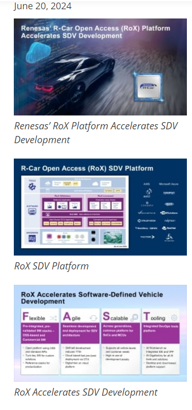
  Renesas Electronics Corporation (TSE:6723), a premier supplier of advanced semiconductor solutions, today launched R-Car Open Access (RoX), a development platform for software-defined vehicles (SDVs) that integrates all essential hardware, operating systems (OS), software and tools needed for automotive developers to rapidly develop next-generation vehicles with secure and continuous software updates. Designed for the Renesas R-Car family of system on chips (SoCs) and microcontrollers (MCUs), the SDV platform includes comprehensive tools for the seamless deployment of AI applications. By pre-integrating all fundamental layers required to develop SDVs, RoX drastically reduces the complexities for car OEMs and Tier 1 suppliers, saving time and money.
Renesas’ R-Car Open Access Platform Accelerates Software-Defined Vehicle Development With Market-Ready Software

  The advent of SDVs represents a major step forward in automotive technology – accelerating toward more driving autonomy, electrification and connected experiences. Cars have to be aware of the 360-degree surrounding space with ASIL D levels of sensing, processing and control to deliver safety and autonomy applications. The in-cabin experiences for drivers and passengers are being revolutionized. As a result, modern electrical/electronics (E/E) architecture depends on software to control vehicle functions, manage real-time data networks across different ECU zones, and provide customer differentiation. It has become more difficult to maintain and upgrade these complex software stacks while ensuring the highest levels of safety. Renesas’ customizable solution solves these challenges by offering a cloud-native development environment and a simulation platform, supporting the software-first approach and parallel hardware and software development.

  Out-of-box Platform with Market-Ready Software Stacks

  The flexible RoX SDV platform is available in two versions. “RoX Whitebox” is an open, easily accessible software package that includes royalty-free OS and hypervisor software such as Android Automotive OS, FreeRTOS, Linux, Xen and Zephyr RTOS, as well as reference applications designed for specific domain systems. “RoX Licensed” is based on industry-proven commercial software solutions, such as QNX and Red Hat In-Vehicle Operating System, as well as AUTOSAR-compliant software and SAFERTOS®. It is pre-integrated and tested to run on Renesas’ R-Car SoCs and MCUs and includes pre-validated software stacks from STRADVISION for Advanced Driver Assistance Systems (ADAS) and Candera CGI Studio for in-vehicle infotainment (IVI), to name a few. These software solutions can be easily productized and customized or expanded depending on OEMs’ needs.

  With the RoX SDV platform, automotive system engineers can start building their software immediately using a highly integrated toolchain even before the hardware is available. This is made possible through the cloud environment and the virtual development platform, which let developers design, debug in simulation, and verify their software before deploying on live SoCs and MCUs. The virtual development platform includes the Renesas Fast Simulator (RFS) as well as partner solutions such as ASTC VLAB VDM and Synopsys Virtualizer Development Kit (VDK) to provide broad coverage of simulation speed, features and use cases.

  For seamless end-to-end AI development, RoX offers the AI Workbench to enable developers to validate and optimize their models and test their AI applications all in the cloud, either on the virtual development platform or on Renesas board farms. A wide range of AI models, automated pipelines, as well as a specific hybrid compiler toolchain (HyCo) are available to support the rapid AI deployment on the R-Car heterogeneous compute platform across generations of SoCs.

  AWS Cloud Services Now Available

  The RoX SDV platform now supports Amazon Web Services (AWS) cloud computing services as part of the AI Workbench development environment. With the Renesas R-Car SDK (Software Development Kit) containerized in the AWS cloud environment, developers can innovate and optimize their designs more efficiently. This tight integration allows them to simulate and test hardware and software combinations instantly and deploy AI applications that seamlessly run on R-Car devices.

  Scalable R-Car Gen 5 Family

  The RoX SDV platform is designed for current generation R-Car SoCs, the upcoming R-Car Gen 5 MCU/SoC Family, and future devices. The SDV platform provides car OEMs and Tier1 suppliers the flexibility to design a broad range of scalable compute solutions for ADAS, IVI, gateway and cross-domain fusion systems as well as body control, domain and zone control systems.

  Renesas’ R-Car Gen 5 is currently the only hardware architecture in the industry that can accommodate the full range of processing requirements – from zonal ECUs to high-end central compute, serving from entry-level vehicles to luxury-class models. Thanks to a new unified hardware architecture based on Arm® CPU cores, customers developing with the R-Car Gen 5 devices will be able to reuse the same software and tools across diverse E/E applications that span car models and generations, preserving their engineering investments. Renesas’ high-performance SoC products will offer both domain-specific and cross-domain solutions using application processing, large display capabilities, sensor connectivity, GPU and AI processing.

  “RoX is a significant advancement that will speed up the shift-left approach for software-defined vehicles,” said Vivek Bhan, Senior Vice President and General Manager of High Performance Computing at Renesas. “Today, car OEMs and Tier1 suppliers are heavily investing in software development and maintenance. Renesas understands this challenge and is closely working with them to deliver a flexible, ready-to-deploy development solution that can be maintained throughout the vehicle’s lifespan. The RoX platform empowers our customers to design vehicles that deliver new value and bring improved safety and delightful comfort experiences to drivers and passengers.”

  “At AWS, we’re committed to helping our customers and partners accelerate development and bring innovation to drivers faster than ever before,” said Andrea Ketzer, Director of Technology Strategy, Automotive & Manufacturing at AWS. “With Renesas’ R-Car Gen 5 devices supported by the AI Workbench on AWS, customers will achieve faster and more validated simulations and the ability to develop independently of hardware. This step change in development will drive the industry forward and place software innovation at the forefront of mobility.”

  According to TechInsights, the market shift to domain, zonal and centralized architectures will translate to a growing processor market, incorporating SoCs and MCUs, worth $25.9 billion by 2031. “Being able to maintain and upgrade complex software stacks that incorporate operating systems, hypervisors and other functional software stacks will thus become an increasingly critical element of the supply chain,” said Asif Anwar, Executive Director of Automotive End Market Research at TechInsights. “By also being able to offer cloud-native environments to support a software-first approach to development and testing of the hardware, the Renesas RoX SDV platform offers a ready-built ecosystem that encompasses these elements in support of a scalable portfolio of next generation R-Car Gen 5 processors to address this sizable market.”

  Renesas’ R-Car Open Access Platform is being demonstrated at the AWS Summit Japan in Tokyo from June 20-21.

  RoX SDV Platform Partners:

  Operating System/Hypervisor Partners

  QNX

  Red Hat

  Vector AUTOSAR

  WITTENSTEIN SAFERTOS®

  Software Stack Partners

  Candera CGI Studio

  EPAM AosEdge

  Excelfore eSync

  MM Solutions

  STRADVISION SVNet

  Nullmax

  Development Tools Partners

  ASTC VLAB Works

  Synopsys Virtualizer Development Kit (VDK)

  Cloud Partners

  AWS

  Microsoft Azure

  Availability

  The R-Car Open Access Platform is available today with the option to license. Open-source OS, commercial OS, full application software stacks, virtual development, cloud infrastructure and debugging and emulation tools are available by Renesas or through partners. Additional information about the development platform is available here and information about the R-Car Gen 5 Family can be found here. Please contact your local sales teams for more details.

("Note: The information presented in this article is gathered from the internet and is provided as a reference for educational purposes. It does not signify the endorsement or standpoint of our website. If you find any content that violates copyright or intellectual property rights, please inform us for prompt removal.")

Online messageinquiry

reading
Renesas Strengthens Power Leadership with New GaN FETs for High-Density Power Conversion in AI Data Centers, Industrial and Charging Systems
  Renesas Electronics Corporation (TSE:6723), a premier supplier of advanced semiconductor solutions, introduced three new high-voltage 650V GaN FETs for AI data centers and server power supply systems including the new 800V HVDC architecture, E-mobility charging, UPS battery backup devices, battery energy storage and solar inverters. Designed for multi-kilowatt-class applications, these 4th-generation plus (Gen IV Plus) devices combine high-efficiency GaN technology with a silicon-compatible gate drive input, significantly reducing switching power loss while retaining the operating simplicity of silicon FETs. Offered in TOLT, TO-247 and TOLL package options, the devices give engineers the flexibility to customize their thermal management and board design for specific power architectures.  The new TP65H030G4PRS, TP65H030G4PWS and TP65H030G4PQS devices leverage the robust SuperGaN® platform, a field-proven depletion mode (d-mode) normally-off architecture pioneered by Transphorm, which was acquired by Renesas in June 2024. Based on low-loss d-mode technology, the devices offer superior efficiency over silicon, silicon carbide (SiC), and other GaN offerings. Moreover, they minimize power loss with lower gate charge, output capacitance, crossover loss, and dynamic resistance impact, with a higher 4V threshold voltage, which is not achievable with today’s enhancement mode (e-mode) GaN devices.  Built on a die that is 14 percent smaller than the previous Gen IV platform, the new Gen IV Plus products achieve a lower RDS(on) of 30 milliohms (mΩ), reducing on-resistance by 14 percent and delivering a 20 percent improvement in on-resistance output-capacitance-product figure of merit (FOM). The smaller die size reduces system costs and lowers output capacitance, which results in higher efficiency and power density. These advantages make the Gen IV Plus devices ideal for cost-conscious, thermally demanding applications where high performance, efficiency and small footprint are critical. They are fully compatible with existing designs for easy upgrades, while preserving existing engineering investments.  Available in compact TOLT, TO-247 and TOLL packages, they provide one of the broadest packaging options to accommodate thermal performance and layout optimization for power systems ranging from 1kW to 10kW, and even higher with paralleling. The new surface-mount packages include bottom side (TOLL) and top-side (TOLT) thermal conduction paths for cooler case temperatures, allowing easier device paralleling when higher conduction currents are needed. Further, the commonly used TO-247 package provides customers with higher thermal capability to achieve higher power.  “The rollout of Gen IV Plus GaN devices marks the first major new product milestone since Renesas’ acquisition of Transphorm last year,” said Primit Parikh, Vice President of the GaN Business Division at Renesas. “Future versions will combine the field-proven SuperGaN technology with our drivers and controllers to deliver complete power solutions. Whether used as standalone FETs or integrated into complete system solution designs with Renesas controllers or drivers, these devices will provide a clear path to designing products with higher power density, reduced footprint and better efficiency at a lower total system cost.”  Unique d-mode Normally-off Design for Reliability and Easy Integration  Like previous d-mode GaN products, the new Renesas devices use an integrated low-voltage silicon MOSFET – a unique configuration that achieves seamless normally-off operation while fully capturing the low loss, high efficiency switching benefits of the high- voltage GaN. As they use silicon FETs for the input stage, the SuperGaN FETs are easy to drive with standard off-the-shelf gate drivers rather than specialized drivers that are normally required for e-mode GaN. This compatibility simplifies design and lowers the barrier to GaN adaptation for system developers.  GaN-based switching devices are quickly growing as key technologies for next-generation power semiconductors, fueled by demand from electric vehicles (EVs), inverters, AI data center servers, renewable energy, and industrial power conversion. Compared to SiC and silicon-based semiconductor switching devices, they provide superior efficiency, higher switching frequency and smaller footprints.  Renesas is uniquely positioned in the GaN market with its comprehensive solutions, offering both high- and low-power GaN FETs, unlike many providers whose success in the field has been primarily limited to lower power devices. This diverse portfolio enables Renesas to serve a broader range of applications and customer needs. To date, Renesas has shipped over 20 million GaN devices for high- and low-power applications, representing more than 300 billion hours of field usage.
2025-07-04 15:04 reading:288
Renesas Sets New MCU Performance Bar with 1-GHz RA8P1 Devices with AI Acceleration
Unprecedented 7300+ CoreMarks1 with Dual Arm CPU coresTSMC 22ULL Process Delivers High Performance and Low Power ConsumptionEmbedded MRAM with Faster Write Speeds and Higher Endurance and RetentionDedicated Peripherals Optimized for Vision and Voice AI plus Real-Time AnalyticsNew AI Software Framework Eases Development and Enables Easy Migration with MPUsLeading-Edge Security Features Ensure Data Privacy  Renesas Electronics Corporation (TSE:6723), a premier supplier of advanced semiconductor solutions, introduced the RA8P1 microcontroller (MCU) Group targeted at Artificial Intelligence (AI) and Machine Learning (ML) applications, as well as real-time analytics. The new MCUs establish a new performance level for MCUs by combining 1GHz Arm® Cortex®-M85 and 250MHz Cortex-M33 CPU cores with the Arm Ethos™-U55 Neural Processing Unit (NPU). This combination delivers the highest CPU performance of over 7300 CoreMarks and AI performance of 256 GOPS at 500 MHz.  Designed for Edge/Endpoint AI  The RA8P1 is optimized for edge and endpoint AI applications, using the Ethos-U55 NPU to offload the CPU for compute intensive operations in Convolutional and Recurrent Neural Networks (CNNs and RNNs) to deliver up to 256 MACs per cycle that yield 256 GOPS performance at 500 MHz. The new NPU supports most commonly used networks, including DS-CNN, ResNet, Mobilenet TinyYolo and more. Depending on the neural network used, the Ethos-U55 provides up to 35x more inferences per second than the Cortex-M85 processor on its own.  Advanced Technology  The RA8P1 MCUs are manufactured on the 22ULL (22nm ultra-low leakage) process from TSMC, enabling ultra-high performance with very low power consumption. This process also enables the use of embedded Magnetoresistive RAM (MRAM) in the new MCUs. MRAM offers faster write speeds along with higher endurance and retention compared with Flash.  “There is explosive growth in demand for high-performance edge AIoT applications. We are thrilled to introduce what we believe are the best MCUs to address this trend,” said Daryl Khoo, Vice President of Embedded Processing Marketing Division at Renesas. “The RA8P1 devices showcase our technology and market expertise and highlight the strong partnerships we have built across the industry. Customers are eager to employ these new MCUs in multiple AI applications.”  “The pace of innovation in the age of AI is faster than ever, and new edge use cases demand ever-improving performance and machine learning on-device,” said Paul Williamson, Senior Vice President and General Manager, IoT Line of Business at Arm. “By building on the advanced AI capabilities of the Arm compute platform, Renesas’ RA8P1 MCUs meet the demands of next generation voice and vision applications, helping to scale intelligent, context-aware AI experiences.”  “It is gratifying to see Renesas harness the performance and reliability of TSMC 22ULL embedded MRAM technology to deliver outstanding results for its RA8P1 devices,” said Chien-Hsin Lee, Senior Director of Specialty Technology Business Development at TSMC. “As TSMC continues to advance our embedded non-volatile memory (eNVM) technologies, we look forward to strengthening our long-standing collaboration with Renesas to drive innovation in future groundbreaking devices.”  Robust, Optimized Peripheral Set for AI  Renesas has integrated dedicated peripherals, ample memory and advanced security to address Voice and Vision AI and Real-time Analytics applications. For vision AI, a 16-bit camera interface (CEU) is included that supports sensors up to 5 megapixels, enabling camera and demanding Vision AI applications. A separate MIPI CSI-2 interface offers a low pin-count interface with two lanes, each up to 720Mbps. In addition, multiple audio interfaces including I2S and PDM support microphone inputs for voice AI applications.  The RA8P1 offers both on-chip and external memory options for efficient, low latency neural network processing. The MCU includes 2MB SRAM for storing intermediate activations or graphics framebuffers. 1MB of on-chip MRAM is also available for application code and storage of model weights or graphics assets. High-speed external memory interfaces are available for larger models. SIP options with 4 or 8 MB of external flash in a single package are also available for more demanding AI applications.  New RUHMI Framework  Along with the RA8P1 MCUs, Renesas has introduced RUHMI (Renesas Unified Heterogenous Model Integration), a comprehensive framework for MCUs and MPUs. RUHMI offers efficient AI deployment of the latest neural network models in a framework agnostic manner. It enables model optimization, quantization, graph compilation and conversion, and generates efficient source code. RUHMI provides native support for machine-learning AI frameworks such as TensorFlow Lite, Pytorch & ONNX. It also provides the necessary tools, APIs, code-generator, and runtime needed to deploy a pre-trained neural network, including ready-to-use application examples and models optimized for RA8P1. RUHMI is integrated with Renesas’s own e2Studio IDE to allow seamless AI development. This integration will facilitate a common development platform for MCUs and MPUs.  Advanced Security Features  The RA8P1 MCUs provide leading-edge security for critical applications. The new Renesas Security IP (RSIP-E50D) includes numerous cryptographic accelerators, including CHACHA20, Ed25519, NIST ECC curves up to 521 bits, enhanced RSA up to 4K, SHA2 and SHA3. In concert with Arm TrustZone®, this provides a comprehensive and fully integrated secure element-like functionality. The new MCUs also provides strong hardware Root-of-Trust and Secure Boot with First Stage Bootloader (FSBL) in immutable storage. XSPI interfaces with decryption-on-the-fly (DOTF) allow encrypted code images to be stored in external flash and decrypted on the fly as it is securely transferred to the MCU for execution.  Ready to Use Solutions  Renesas provides a wide range of easy-to-use tools and solutions for the RA8P1 MCUs, including the Flexible Software Package (FSP), evaluation kits and development tools. FreeRTOS and Azure RTOS are supported, as is Zephyr. Several Renesas software example projects and application notes are available to enable faster time to market. In addition, numerous partner solutions are available to support development with the RA8P1 MCUs, including a driver monitoring solution from Nota.AI and a traffic/pedestrian monitoring solution from Irida Labs. Other solutions can be found at the Renesas RA Partner Ecosystem Solutions Page.  Key Features of the RA8P1 MCUs  Processors: 1GHz Arm Cortex-M85, 500MHz Ethos-U55, 250 MHz Arm Cortex-M33 (Optional)  Memory: 1MB/512KB On-chip MRAM, 4MB/8MB External Flash SIP Options, 2MB SRAM fully ECC protected, 32KB I/D caches per core  Graphics Peripherals: Graphics LCD controller supporting resolutions up to WXGA (1280x800), parallel RGB and MIPI-DSI display interfaces, powerful 2D Drawing engine, parallel 16bit CEU and MIPI CSI-2 camera interfaces, 32bit external memory bus (SDRAM and CSC) interface  Other Peripherals: Gigabit Ethernet and TSN Switch, XSPI (Octal SPI) with XIP and DOTF, SPI, I2C/I3C, SDHI, USBFS/HS, CAN-FD, PDM and SSI audio interfaces, 16bit ADC with S/H circuits, DAC, comparators, temperature sensor, timers  Security: Advanced RSIP-E50D cryptographic engine, TrustZone, Immutable storage, secure boot, tamper resistance, DPA/SPA attack protection, secure debug, secure factory programming, Device Lifecycle management  Packages: 224BGA, 289BGA
2025-07-04 14:56 reading:274
Renesas:Enhance HMI User Experience with Built-in Large Memory MPU
  The HMI market continues to drive growth in better user experience and increased automation with the expansion of HMI applications. This results in a strong demand for improved functionality and performance in display-based applications, such as real-time plotting, smooth animation, and USB camera image capture, in affordable systems. Microprocessors (MPUs) with high-speed, large-capacity built-in memory that can be used like microcontrollers (MCUs) are gaining attention in the market. Renesas' RZ/A3M MPU with a built-in 128MB DDR3L SDRAM and a compatible package for a two-layer PCB design is the ideal solution for realizing smooth animation and high-quality HMI at a reasonable system cost.  High-Performance HMI and Real-Time Graphics  Integrating high-speed, large-capacity memory directly into the MPU package offers several advantages, including mitigating concerns about high-speed signal noise on the PCB and simplifying PCB design for the users. The large-capacity memory needed for high-performance HMIs is externally connected to the MPU in the conventional way. Additionally, PCBs equipped with DDR memory and high-speed signal interfaces require multi-layer PCB designs to account for signal noise, making it challenging to reduce PCB costs. Also, the common capacity of on-chip SRAM is typically between 1MB and 10MB, which is too small for high-performance HMIs that need to include a reasonable number of tasks in the near future. To overcome these issues, Renesas released an industry-leading RZ/A3M MPU with a large built-in 128MB DDR3L memory to support high-performance HMI and real-time graphics performance to enhance better and faster user experiences. Most importantly, the board does not require a high-speed signal interface and supports two-layer PCB design to reduce board noise and simplify system development for users.Figure 1. Strengths of Built-in DDR Memory  Designing High-Performance PCBs at a Reasonable System Cost  The number of PCB layers and the ease of design significantly impact the cost of system implementation and maintenance in user applications. As shown in Figure 2, using a wide pin pitch of 0.8mm allows for the layout of signal lines and placement of VIAs between the balls. Additionally, placing the balls handling the main signals in the outer rows of the 244-pin 17mm x 17mm LFBGA package and positioning the GND and power pins as inner balls allows for efficient routing of the necessary signal lines for the system (Figure 3). The RZ/A3M MPU is designed to build cost-effective systems with two-layer PCBs through its innovative packaging and pin assignments.Figure 2. Signal Wiring and Ball LayoutImageFigure 3. Optimized Ball Arrangement for a Two-Layer Board Layout  User-Friendly Interface Enabling Smooth GUI Display  The high-resolution graphic LCD controller integrated into the RZ/A3M supports both parallel RGB and 4-lane MIPI-DSI interfaces, accommodating displays up to 1280x800. Additionally, the 2D graphics engine, high-speed 16-bit 1.6Gbps DDR3L memory, and 1GHz Arm® Cortex®-A55 CPU enable high-performance GUI displays, including smooth animations and real-time plotting that increase the possibility of automation in HMI applications. Connecting a USB camera to the USB 2.0 interface enables smooth capture of camera images, making it easy to check inside of an apparatus, for example, the doneness of the food in the oven or the condition in the refrigerator.  The EK-RZ/A3M is an evaluation kit for the RZ/A3M. It includes an LCD panel with a MIPI-DSI interface. With this kit, users can immediately start evaluation. Renesas also has several graphics ecosystem partners – LVGL, SquareLine Studio, Envox, Crank, RTOSX – who deliver GUI solutions utilizing the EK-RZ/A3M to further accelerate your development cycle.Figure 4. High-Definition HMI Example with the EK-RZ/A3M  The RZ/A3M MPU, equipped with high-speed 128MB DDR3L memory and a 1GHz Arm Cortex-A55, excels in developing cost-effective HMI applications with real-time plot UIs, smooth animations, and USB camera capture. The integrated memory simplifies PCB design by removing the need for high-speed signal interface design. Visit www.renesas.com/rza3m to learn more about the technical details and how to start developing the next HMI applications for consumer electronics, smart home, building automation, healthcare, industrial applications, and office automation.
2025-06-06 15:27 reading:397
Renesas Extends RZ/A MPU Line-up with RZ/A3M for Cost-Sensitive, Advanced HMI Solutions
  Renesas Electronics Corporation (TSE:6723), a premier supplier of advanced semiconductor solutions, today introduced a new high-performance microprocessor (MPU) in the RTOS-based RZ/A series that meets the growing demands of advanced human-machine interface (HMI) systems. The new RZ/A3M MPU comes with large SDRAM, SRAM and RTOS support to facilitate the seamless execution of complex tasks and real-time graphical displays. The RZ/A3M drives video and camera output on large LCD panels with resolutions up to 1280x800, addressing the display requirements in next-generation home appliances, industrial and office automation, healthcare devices and building control systems.  Similar to its existing RZ/A3UL, the RZ/A3M features a 64-bit Arm® Cortex®-A55 core with a maximum operating frequency of 1 GHz and 128 KB (kilobytes) of on-chip SRAM. By integrating high-speed 128MB DDR3L-SDRAM in a single System-in-Package (SiP), the device eliminates the complex task of designing a high-speed signal interface for connecting external memory.  Reducing System Cost with Built-in Memory and Simplified PCB Design  The RZ/A3M is designed to reduce system costs and accelerate development. It supports both external NAND and NOR flash via QSPI for data and code storage. Paired with a driver, high-capacity NAND flash offers a cost-effective option for memory expansion. Additionally, the RZ/A3M's BGA package has a unique pin layout with two main rows positioned on the outside edge. This layout simplifies PCB routing and enables a low-cost, dual-layer printed wiring board design, providing significant cost and time savings. This memory integration simplifies PCB design by reducing the routing complexity and minimizing layout constraints.  “I’m pleased to launch the RZ/A3M, the first RZ product with large built-in memory targeting high-function video/animation HMI performance while keeping overall system costs low,” said Daryl Khoo, Vice President of the Embedded Processing Marketing Division at Renesas. “In addition, we aim to deliver a highly responsive user experience with high-quality, real-time graphics, and provide the ease of design and cost efficiency to help our customers build advanced HMI solutions quickly.”  Comprehensive Development Environment  Renesas offers a comprehensive HMI development environment that includes the Flexible Software Package (FSP), evaluation kits, development tools, and sample software. Graphical user interface (GUI) solutions from partner companies such as LVGL, Crank, SquareLine Studio, and Envox will be available for the RZ/A3M to facilitate rapid HMI graphics development.  Key Features of RZ/A3M  Arm Cortex-A55 CPU with a maximum operating frequency of 1GHz  128KB SRAM with error correction, Built-in 128MB DDR3L SDRAM  Graphics capabilities: LCD controller supporting resolutions up to 1280x800 (WXGA), parallel RGB and MIPI-DSI (4-lane) interfaces, 2D graphics drawing engine  Peripheral functions: QSPI interface for serial NOR/NAND flash memory, SPI, I2C, SDHI, USB2.0, I2S, temperature sensor, timer  Package: 244-pin LFBGA, 17mm x 17mm, 0.8mm pitch  Renesas’ Comprehensive HMI Solutions  Renesas offers a wide variety of HMI solutions ranging from the 32-bit RX and RA MCU families to the 64-bit RZ family supporting 4K displays. The RZ/A series, built on RTOS-based MPUs with fast startup, includes the new RZ/A3M, which delivers high-performance HMI capabilities with the same ease of use offered by MCUs using large memory capacity.  Multi-HMI Winning Combination  Renesas offers Multi-HMI Solution which combines the new RZ/A3M MPU with numerous compatible devices from its portfolio to offer HMI functions for appliances. These Winning Combinations are technically vetted system architectures from mutually compatible devices that work together seamlessly to bring an optimized, low-risk design for faster time to market. Renesas offers more than 400 Winning Combinations with a wide range of products from the Renesas portfolio to enable customers to speed up the design process and bring their products to market more quickly. They can be found at renesas.com/win.
2025-05-26 14:49 reading:433
  • Week of hot material
  • Material in short supply seckilling
model brand Quote
MC33074DR2G onsemi
RB751G-40T2R ROHM Semiconductor
TL431ACLPR Texas Instruments
BD71847AMWV-E2 ROHM Semiconductor
CDZVT2R20B ROHM Semiconductor
model brand To snap up
STM32F429IGT6 STMicroelectronics
ESR03EZPJ151 ROHM Semiconductor
BU33JA2MNVX-CTL ROHM Semiconductor
TPS63050YFFR Texas Instruments
BP3621 ROHM Semiconductor
IPZ40N04S5L4R8ATMA1 Infineon Technologies
Hot labels
ROHM
IC
Averlogic
Intel
Samsung
IoT
AI
Sensor
Chip
About us

Qr code of ameya360 official account

Identify TWO-DIMENSIONAL code, you can pay attention to

AMEYA360 weixin Service Account AMEYA360 weixin Service Account
AMEYA360 mall (www.ameya360.com) was launched in 2011. Now there are more than 3,500 high-quality suppliers, including 6 million product model data, and more than 1 million component stocks for purchase. Products cover MCU+ memory + power chip +IGBT+MOS tube + op amp + RF Bluetooth + sensor + resistor capacitance inductor + connector and other fields. main business of platform covers spot sales of electronic components, BOM distribution and product supporting materials, providing one-stop purchasing and sales services for our customers.

Please enter the verification code in the image below:

verification code