NOVOSENSE Launches NSIP3266 Full-Bridge Transformer Driver with Integrated Crystal Oscillator, Simplifying Isolated Driver Power Supply Design

发布时间:2025-02-19 09:59
作者:AMEYA360
来源:NOVOSENSE
阅读量:1309

  NOVOSENSE today announced the launch of the NSIP3266 full-bridge transformer driver with integrated crystal oscillator, multiple protection functions and soft start support, which can be widely used in isolated driver power supply circuits in automotive on-board chargers (OBCs), traction inverters and charging piles, photovoltaic power generation and energy storage, server power supply and other systems. NSIP3266 supports a full-bridge topology with a wide range of inputs, and with clever pin and function design, it greatly simplifies the design of isolated driver’s power supply circuits, facilitating system manufacturers to optimize system circuits and shorten product time to market.

NOVOSENSE Launches NSIP3266 Full-Bridge Transformer Driver with Integrated Crystal Oscillator, Simplifying Isolated Driver Power Supply Design

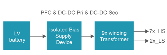
  Currently, isolated driver's power supply in high-voltage systems is available in three architectural forms: centralized, fully distributed, and semi-distributed. Centralized architecture has only one stage of power supply, and the auxiliary power input voltage has a wide input range, requiring closed-loop operation. At the same time, the transformer design is complicated, and especially when a single low-cost isolated power supply is used, there are problems of multi-output load regulation and long wiring, which increase the difficulty of system design and debugging.
NOVOSENSE Launches NSIP3266 Full-Bridge Transformer Driver with Integrated Crystal Oscillator, Simplifying Isolated Driver Power Supply Design

  Fully distributed architecture uses independent isolated power modules to supply power to isolated drivers. The advantage is that 1-to-1 power supply and targeted protection can be achieved for isolated drivers, but a corresponding number of isolated power modules need to be configured, and the system cost is high.

NOVOSENSE Launches NSIP3266 Full-Bridge Transformer Driver with Integrated Crystal Oscillator, Simplifying Isolated Driver Power Supply Design

  Semi-distributed architecture adopts a balanced strategy. Through a two-stage auxiliary power architecture, the first stage uses devices with a wide input voltage range to generate regulated rails, and the second stage can be a compact open-loop form using other devices to provide isolated power supply for isolated drives. Semi-distributed architecture is gaining popularity among engineers because of its simplicity in design and balance of system cost, performance, and protection requirements.

NOVOSENSE Launches NSIP3266 Full-Bridge Transformer Driver with Integrated Crystal Oscillator, Simplifying Isolated Driver Power Supply Design

  Simplified circuit design with full-bridge topology

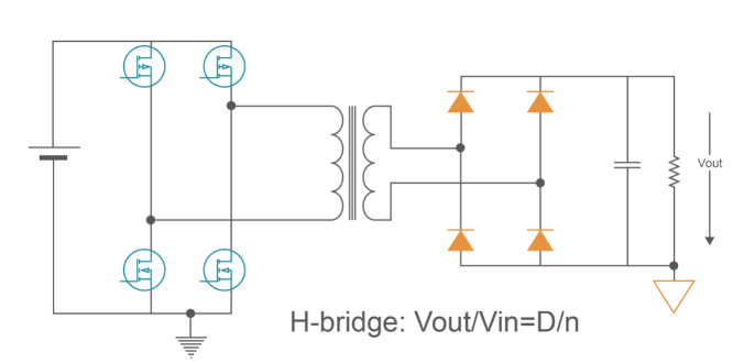
  NOVOSENSE's NSIP3266 full-bridge transformer driver is designed for semi-distributed architecture with isolated driver power supply. Common topology options for semi-distributed architecture include push-pull, LLC, and full-bridge. NSIP3266 adopts full-bridge topology. Compared with other solutions, the principle of full-bridge topology is simple, the transformer structure does not require a center tap, the working principle does not involve the design and selection of external L and C, and the peripheral BOM is often minimal. At the same time, the full-bridge topology is more tolerant to transformer design, including leakage inductance and parasitics, which saves engineers' efforts in system design and debugging.
NOVOSENSE Launches NSIP3266 Full-Bridge Transformer Driver with Integrated Crystal Oscillator, Simplifying Isolated Driver Power Supply Design

  Ingenious design releases MCU resources

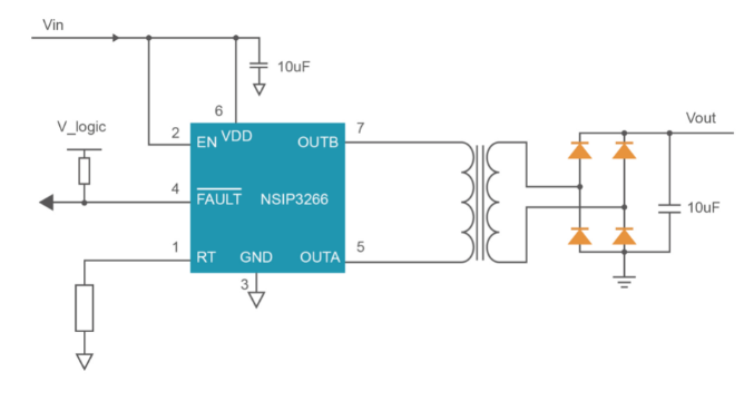
  It is worth mentioning that NSIP3266, through the internal integrated crystal oscillator circuit and RT pin design, allows engineers to complete the switching frequency configuration with only external resistors, achieving decoupling of MCU control and more flexible layout. At the same time, it can still provide safe power supply when the MCU fails, promoting higher system safety. In addition, the built-in soft-start function of NSIP3266 also eliminates the need for MCU control. While not requiring MCU domain routing, it saves secondary-side current limiting resistors, greatly simplifying board design and improving architectural flexibility.
NOVOSENSE Launches NSIP3266 Full-Bridge Transformer Driver with Integrated Crystal Oscillator, Simplifying Isolated Driver Power Supply Design

  Wide voltage input and comprehensive protection

  NSIP3266 supports a wide operating voltage range of 6.5V~26V. No additional TVS protection tube is required in the system circuit, allowing engineers to choose the pre-stage power supply more flexibly. In addition, NSIP3266 provides multiple protection functions, including undervoltage protection, overcurrent protection, over-temperature protection, etc. The comprehensive protection functions enable engineers to focus on the optimization and innovation of the core system functions, and to design the system quickly and efficiently to meet the reliability requirements.

  Packaging and selections

  NSIP3266 is available in EP-MSOP8 package (3.0 x 3.0mm x 0.65mm, with thermal pad). The industrial version, NSIP3266-D, and the automotive version, NSIP3266-Q1, which meets the requirements of AEC-Q100, will be mass-produced in the first half of 2025. Please contact NOVOSENSE's sales team (sales@novosns.com) for product details or to request samples.

  Rich isolation products meet diverse needs

  With its expertise and leadership in isolation technology, NOVOSENSE provides a series of isolation and "isolation+" products covering digital isolators, isolated sampling, isolated interfaces, isolated power supply, and isolated drivers. NSIP3266 is a new addition to NOVOSENSE's isolated power supply family. NOVOSENSE also offers a selection of other cost-effective and high-performance, high-integration options, including: the NSIP605x series of push-pull transformer drivers; the NSIP88/89xx and NIRSP31x series with integrated transformers and multi-channel digital isolators; the NSIP83086 isolated RS485 transceiver and the NSIP1042 isolated CAN transceiver with integrated transformers and isolated interfaces. NOVOSENSE's comprehensive "isolation+" product portfolio can meet the diverse system design needs of various types of customers and provide one-stop chip solutions for them.

(备注:文章来源于网络,信息仅供参考,不代表本网站观点,如有侵权请联系删除!)

在线留言询价

相关阅读
NOVOSENSE launches NSUC1612: Fully Integrated Embedded Motor Drive SoC for Smarter, Cost-Efficient Automotive Actuators
  NOVOSENSE has released the NSUC1612, a next-generation motor driver SoC designed to address the limitations of traditional discrete solutions in automotive smart actuators, such as system complexity, high cost, and limited reliability.  With its fully integrated single-chip architecture, the NSUC1612 can simplify design, reduce cost, and enhance stability. It supports a wide range of applications, including automotive water valves, automotive air-conditioning vent, active grille shutters, as well as stepper motors, DC brushed motors, and DC brushless motors—delivering an efficient and scalable solution for automotive electronics.  1.Fully Integrated Architecture: Simplified Design, Reduced Complexity  Conventional actuator control systems often require multiple components, including MCU, motor drivers, communication interfaces, and protection circuits, leading to complex PCB layout, increased solder joints, and compatibility issues.The NSUC1612 integrates a 32-bit ARM® Cortex®-M3 MCU with 4- or 3-channel half-bridge drivers, LIN/CAN controller communication interfaces, a 12-bit ADC, temperature sensors, and other essential modules, all in a single-chip. This eliminates the need for additional companion ICs while covering the full motor control, communication, and protection process.By reducing external components and simplifying hardware design, the NSUC1612 shortens development cycles and minimizes EMI risk through optimized internal signal routing.  2.Excellent EMC Performance: Reliable Operation in Harsh Environments  Automotive electronics operate in complex electromagnetic conditions where EMC performance directly impacts actuator precision and system stability. The NSUC1612 provides simplified reference circuits and optimized PCB layout. In compliance with CISPR 25:2021 Class 5, it passes stringent automotive EMC/EMI tests, compliant with the automotive standardsSelected Test Results Based on CISPR 25:2021  This ensures stable motor control signals and helps prevent malfunctions such as actuator stalls or misoperation caused by electromagnetic interference.  3.Strong Performance: Balanced Drive Capability and Processing Power  The NSUC1612 is designed to deliver both reliable motor driving capability and efficient computation: NSUC1612B: 4 half-bridge outputs, peak current up to 500 mA NSUC1612E: 3 half-bridge outputs, peak current up to 2.1 AThese options support brushed DC, BLDC, and stepper motors across diverse applications, from HVAC air vent adjustment to seat ventilation.  The ARM® Cortex®-M3 core with Harvard architecture integrates 32 KB Flash, 2 KB SRAM, and 15 KB ROM with Bootloader, supporting OTA upgrades. A 32 MHz high-precision oscillator with PLL ensures stable computation, while low-power sleep mode consumes less than 50 μA across the full operation temperature range, balancing performance with energy efficiency.  4.Automotive-Grade Reliability: Built for Demanding Conditions  The NSUC1612 is designed with comprehensive reliability features to withstand harsh operating environments. It is compliant with AEC-Q100 Grade 1, supporting junction temperatures up to 150°C and ensuring stable operation across a wide temperature range from -40°C to +125°C. The device’s LIN port can tolerate up to ±40 V, while the BVDD pin supports -0.3 V to 40 V, enabling direct connection to 12V automotive batteries. In addition, integrated protection mechanisms such as over-voltage and over-temperature safeguards provide robust defense against voltage fluctuations and transient surges, delivering system-level reliability under real-world automotive conditions.  The NSUC1612 extends its value through broad application compatibility, making it suitable for automotive actuator systems. It supports brushed DC, BLDC, and stepper motors, while integrated communication interfaces—including LIN PHY (compliant with LIN 2.x, ISO 17987, and SAE J2602), FlexCAN, and SPI—allow seamless integration into existing automotive network architectures.  The NSUC1612 is ideal for a wide range of applications, including thermal management components (e.g., automotive water valves and expansion valves), cabin comfort modules (automotive air-conditioning vent), and smart body systems (active grille shutters and charging port actuators). By integrating these functions into a single device, it helps reduce design costs and simplify development.
2025-09-23 13:12 阅读量:440
Adapting to challenging magnetic environments: MT73xx 3D dual-output Hall latches from NOVOSENSE enable precise automotive motor control
  The NOVOSENSE MT73xx series dual-output Hall latches, based on 3D Hall technology, support SS (Speed & Speed) or SD (Speed & Direction) dual-channel outputs and complies with Automotive Grade 0 standards. Ideal for motor control systems such as power windows, liftgates, and sunroofs, this product family enhances the accuracy and stability of speed and position detection, optimizing overall in-vehicle comfort.  In motor control systems, precise detection of speed and direction signals directly influences system response speed and operational stability. Traditional solutions typically rely on a combination of two separate Hall latches, requiring high magnetic ring installation precision. This often leads to issues such as signal phase deviation, poor synchronization, and structural complexity.  Integrates a 3D Hall sensing structure with inherent orthogonal output characteristics, the MT73xx series can simultaneously deliver dual-channel speed signals (SS output) with a 90° phase difference or speed and direction signals (SD output), making it widely suitable for “speed-direction” detection applications. This design reduces dependency on precise positioning of magnetic poles, mitigates dual-channel phase deviation, simplifies system architecture, and improves overall system stability, providing a more flexible and reliable solution for motion control detection.  Compatibility with diverse magnetic ring configurations enabled by VHS technology  To achieve high-precision 3D sensing, the MT73xx series adopts NOVOSENSE’s proprietary VHS (Vertical Hall Sensor) technology. Through combinations of XY, YZ, and XZ axial sensing, any two axes naturally deliver orthogonal outputs, enhancing signal synchronization.  Additionally, the MT73xx series offers excellent compatibility with various magnetic ring configurations – whether axial, radial, or irregularly shaped magnets – maintaining robust duty cycle performance. This allows customers to adapt designs flexibly depending on magnetic ring characteristics and installation environments, further reducing development complexity and tuning costs.  Dual-output design for optimized system integration  Regarding system integration, the MT73xx’s dual-output capability allows it to replace traditional single- or dual-Hall solutions by directly transmitting SS (Speed & Speed) or SD (Speed & Direction) signals to ECU, minimizing the requirements for peripheral redundant position sensors.  This approach not only saves PCB space and simplifies structural layouts, but also enhances solution integration, offering greater design flexibility for innovative applications in motor control and intelligent cockpit systems.
2025-08-13 15:35 阅读量:657
High-voltage half-bridge driver NSD2622N from NOVOSENSE: A high-reliability, high-integration solution tailored for E-mode GaN
  NOVOSENSE has launched NSD2622N, a high-voltage half-bridge driver IC specifically designed for enhancement-mode GaN (E-mode GaN). This chip integrates positive/negative voltage regulation circuits, supports bootstrap supply, and provides high dv/dt immunity and robust driving capability. It significantly simplifies GaN driver circuit design while enhancing system reliability and reducing overall costs.  Application background  In recent years, gallium nitride high-electron-mobility transistors (GaN HEMTs) are gaining increasingly widespread adoption in high-voltage, high-power applications, such as AI data center power supplies, microinverters, and on-board chargers (OBCs). With significant advantages of high switching frequency and low switching losses, GaN HEMTs enable substantially improved power density in power supply systems, noticeably optimized energy efficiency, and significantly reduced system costs.  However, GaN devices still face challenges in real-world applications. For instance, E-mode GaN devices exhibit low turn-on thresholds. In high-voltage and high-power applications, particularly in hard-switching operation mode, poorly designed driver circuits can lead to false triggering due to crosstalk during high-frequency high-speed switching. Additionally, the complexity of compatible driver circuit designs raises the barrier to GaN device adoption.  To accelerate widespread GaN adoption, leading GaN manufacturers at home and abroad have introduced some power ICs with integrated drivers, especially MOSFET-LIKE GaN power devices in Si-MOSFET-compatible packages, which somewhat reduce GaN driver circuit design complexity. However, driver-integrated GaN solutions have limitations: they struggle to meet customized design requirements and are unsuitable for applications adopting multi-device parallel or bidirectional switching topologies. Therefore, discrete GaN devices with dedicated drivers remain essential for many applications. To address the above-mentioned limitations, NOVOSENSE has developed NSD2622N – a driver IC tailored to E-mode GaN, aiming to deliver high-performance, high-reliability, and cost-competitive driving solutions for high-voltage and high-power GaN applications.  Product features  NSD2622N is a high-voltage half-bridge driver IC specifically designed for E-mode GaN. It integrates a voltage regulation circuit capable of generating a configurable stable positive voltage from 5V to 6.5V to ensure reliable GaN driving, as well as a charge pump circuit that produces a fixed -2.5V negative voltage for reliable GaN turn-off. By integrating both positive and negative voltage regulation circuits, the chip supports high-side output with bootstrap supply.  NSD2622N leverages NOVOSENSE’s proven capacitive isolation technology. Its high-side driver withstands a voltage range of -700V to +700V and a minimum SW dv/dt immunity of 200V/ns. Meanwhile, low propagation delay and tight delay matching between high-side and low-side outputs make it a perfect match for the high-frequency, high-speed switching requirements of GaN devices. Additionally, NSD2622N delivers 2A (source) and -4A (sink) peak drive currents on both high-side and low-side outputs, meeting the requirements of high-speed GaN driving and multi-device parallel configurations. The IC also includes an integrated 5V LDO that can power circuits like digital isolators in applications requiring isolation.  Key specifications of NSD2622N  SW voltage range: -700V to 700V  SW dv/dt immunity: > 200V/ns  Wide supply voltage range: 5V-15V  Adjustable positive output voltage range: 5V-6.5V  Built-in negative output voltage: -2.5V  Peak drive current: 2A (source) / 4A (sink)  Minimum input pulse width (typical): 10ns  Input-to-output propagation delay (typical): 38ns  Pulse width distortion (typical): 5ns  Rise time (1nF load, typical): 6.5ns  Fall time (1nF load, typical): 6.5ns  Built-in dead time (typical): 20ns  Bootstrap supply for high-side output  Integrated 5V LDO for digital isolator supply  Undervoltage lockout (UVLO) and overtemperature protection  Operating temperature range: -40°C to +125°CFunctional block diagram of NSD2622N  Eliminating false triggering risks and providing more stable drive voltage  Compared to conventional Si MOSFET driver solutions, the key challenge in E-mode GaN driver circuit design lies in providing appropriate, stable and reliable positive/negative bias voltages. This is because that E-mode GaN typically requires a 5V-6V turn-on voltage, while its threshold voltage is as low as 1V, or even lower at high temperatures, necessitating negative turn-off voltage to prevent false triggering. To address this challenge, two common drive solutions are used for E-mode GaN: resistive-capacitive (RC) voltage division drive and direct drive.  1. RC voltage division drive  This approach utilizes standard Si MOSFET driver ICs. As shown in the diagram, during turn-on, the parallel combination of Cc and Ra is connected with Rb in series, dividing the driver supply voltage (e.g., 10V) to provide a 6V gate drive voltage for the GaN device, with Dz1 clamping the positive voltage. During turn-off, Cc discharges to provide negative turn-off voltage for the GaN device, with Dz2 clamping the negative voltage.RC voltage division drive solution  Although the RC voltage division circuit does not require sophisticated driver ICs, it introduces additional parasitic inductance due to a large number of components involved, which can impact GaN’s switching performance at high frequencies. Moreover, since the negative turn-off voltage relies on discharge from capacitor Cc, the negative turn-off voltage proves unreliable.  As shown in the half-bridge demo board test waveforms, during the startup phase (T1 in the waveform), the absence of initial charge on Cc results in failure to establish negative voltage and thus zero-voltage turn-off; during the negative turn-off period following the driver’s signal transmission (T2), the negative voltage amplitude fluctuates with capacitor discharge; and during the prolonged turn-off period (T3), the capacitor cannot sustain negative voltage, eventually discharging to zero. Consequently, RC voltage division circuits are generally limited to medium/low power applications with relatively lower reliability requirements, and are proved unsuitable for high-power systems.Waveform of E-mode GaN using RC voltage division drive circuit(CH2: Drive supply voltage; CH3: GaN gate-source voltage)  2. Direct drive  The direct drive solution requires selecting a driver IC with an appropriate undervoltage-lockout (UVLO) threshold, for example, NSI6602VD, which is specifically designed for E-mode GaN with a 4V UVLO threshold. When paired with an external positive/negative voltage regulation circuit, it can directly drive E-mode GaN devices. Below is a typical application circuit.NSI6602VD driver circuitPositive and negative voltage regulation circuits  This direct drive solution can provide reliable negative turn-off voltage for GaN under all operating conditions, when the auxiliary power supply is functioning normally. As a result, this approach is widely adopted in various high-voltage, high-power GaN applications.  The next-generation GaN driver NSD2622N from NOVOSENSE, integrates the positive/negative voltage regulation circuits directly into the chip. As shown in the half-bridge demo board test waveforms below, NSD2622N maintains consistent negative turn-off voltage amplitude and duration regardless of operating conditions. Specifically, during startup (T1 in the waveform), the negative voltage is established even before the driver sends signals; during GaN turn-off (T2), the negative voltage remains stable in amplitude; during extended periods without driver signals (T3), the negative voltage continues to stay reliably stable.Waveforms of E-mode GaN using NSD2622N driver circuit(CH2: Low-side GaN Vds, CH3: Low-side GaN Vgs)  Simplified circuit design and reduced system costs  NSD2622N can provide stable and reliable direct drive for GaN devices. More importantly, by integrating positive/negative voltage regulators, it significantly reduces external component count. By adopting the bootstrap supply architecture, NSD2622N greatly simplifies driver power circuit design and lowers overall system costs.  Taking a 3kW power supply unit (PSU) as an example, assuming both phases of the interleaved TTP PFC and full-bridge LLC use GaN devices, a complexity comparison between two direct-drive solutions is given below:  When using the NSI6602VD driver solution, each half-bridge high-side driver requires an independent isolated power supply in conjunction with corresponding isolation and positive/negative voltage regulation circuits. This means complex auxiliary power supply design for isolation. Given the high power quality requirements of GaN driving and the fact that the main power paths of the PFC and LLC stages are typically placed on separate boards, a two-stage auxiliary power architecture is often necessary. In this configuration, the first stage typically employs a device with wide input voltage range like flyback converter, to generate regulated voltage rails. The second stage may use an open-loop full-bridge topology to provide isolated power and further regulate the power to generate the required positive and negative supply voltages for NSI6602VD. Below is a typical power architecture for such a driver solution.Typical power architecture for NSI6602VD driver solution  The NSD2622N driver solution significantly simplifies auxiliary power design through its bootstrap supply capability. Below is a typical power architecture for this approach.Typical power architecture for NSD2622N driver solution  A detailed comparison of bill-of-materials (BOM) for driver and power supply circuits between the above-mentioned two GaN direct-drive solutions is provided in the table below. It can be seen that the NSD2622N solution utilizing bootstrap supply, dramatically reduces total component count compared to the NSI6602VD’s isolated power supply approach, resulting in substantially lower system costs. Even in applications requiring isolated power supply, NSD2622N maintains its competitive edge - its integrated positive/negative voltage regulators enable a more simplified peripheral circuit relative to the NSI6602VD solution, leading to fewer components and lower system costs.BOM comparison between two GaN direct drive solutions  Versatile GaN compatibility and flexible drive voltage adjustment  The E-mode GaN driver IC NSD2622N from NOVOSENSE delivers not only superior performance but also broad compatibility across various GaN devices from different brands, of different types (including both voltage-mode and current-mode), and at different voltage ratings. For instance, the output voltage of NSD2622N can be set between 5V to 6.5V by adjusting feedback resistors. This enables selection of the most appropriate driving voltage for any GaN device by simply adjusting the feedback resistors to match specific GaN characteristics, allowing GaN devices from different brands to operate at their individual peak performance points.  In addition, NSD2622N features a minimum dv/dt immunity of 200V/ns on the switching node (SW), enhancing the upper limit of GaN switching speed. The adoption of a more compact QFN package and the design of independent turn-on and turn-off output pins further reduce the driver loop parasitic inductance. The over-temperature protection ensures safer GaN applications.  NOVOSENSE also offers single-channel GaN driver IC NSD2012N. Featuring 3mm*3mm QFN package and adjustable negative voltage capability, it can meet more personalized application requirements.
2025-08-07 14:08 阅读量:690
NOVOSENSE Launches High-Performance 2-Wire Hall Switch MT72xx Series: Compact Design with System-Level Reliability
  NOVOSENSE Microelectronics ("NOVOSENSE") has launched the MT72xx series, 2-wire current output Hall switches. The switches feature superior EMC performance, multiple sensing polarity options, and highly integrated design, achieving ASIL-A functional safety certification and full compliance with AEC-Q100 Grade 0 standards. Designed for long-wiring scenarios in vehicle body electronics and domain controller systems, the MT72xx series provides optimized solutions for seatbelt buckle detection, window lift motor control, and other automotive applications.  Addressing Long Wiring Harness Challenges in Automotive  With rapid advancement of automotive intelligence and electrification, increasingly complex vehicle body functions and highly integrated domain controllers have significantly extended wiring harnesses between sensors and control units. This introduces critical challenges including elevated signal interference risks, increased costs, and compromised system reliability.  NOVOSENSE's MT72xx series delivers robust signal integrity while effectively reducing wiring complexity and lowering harness costs. Designed for long-wiring scenarios such as door lock detection, anti-pinch window control, power tailgate position sensing, seat adjustment, and seatbelt buckle detection, these devices provide stable current output with superior anti-interference capabilities, maintaining signal reliability even in extended wiring conditions.  High Integration & Robustness for Automotive-Grade Standards  Engineered for harsh automotive environments with strong EMI interference, the MT72xx series integrates a 100nF(only TO92S package)capacitor to enhance EMC/ESD performance, simplify peripheral configuration, and optimize BOM space, enabling flexible system architecture design. Compliant with AEC-Q100 Grade 0, the devices ensure long-term stability under extreme high-temperature conditions.  Featuring multiple sensing polarity options (unipolar, omnipolar, latch) and adjustable sensitivity thresholds, the MT72xx series offers design flexibility to accommodate diverse magnet solutions and vehicle architectures, streamlining development and debugging processes.  Comprehensive Resources to Accelerate Time-to-Market  To expedite customer development, NOVOSENSEN provides dedicated MT72xx demo boards and magnetic simulation services. These resources enable rapid device validation, magnet solution matching, and cost-effective debugging, significantly shortening product deployment cycles.
2025-07-14 14:25 阅读量:681
  • 一周热料
  • 紧缺物料秒杀
型号 品牌 询价
BD71847AMWV-E2 ROHM Semiconductor
CDZVT2R20B ROHM Semiconductor
TL431ACLPR Texas Instruments
RB751G-40T2R ROHM Semiconductor
MC33074DR2G onsemi
型号 品牌 抢购
ESR03EZPJ151 ROHM Semiconductor
STM32F429IGT6 STMicroelectronics
TPS63050YFFR Texas Instruments
BP3621 ROHM Semiconductor
BU33JA2MNVX-CTL ROHM Semiconductor
IPZ40N04S5L4R8ATMA1 Infineon Technologies
热门标签
ROHM
Aavid
Averlogic
开发板
SUSUMU
NXP
PCB
传感器
半导体
相关百科
关于我们
AMEYA360微信服务号 AMEYA360微信服务号
AMEYA360商城(www.ameya360.com)上线于2011年,现 有超过3500家优质供应商,收录600万种产品型号数据,100 多万种元器件库存可供选购,产品覆盖MCU+存储器+电源芯 片+IGBT+MOS管+运放+射频蓝牙+传感器+电阻电容电感+ 连接器等多个领域,平台主营业务涵盖电子元器件现货销售、 BOM配单及提供产品配套资料等,为广大客户提供一站式购 销服务。

请输入下方图片中的验证码:

验证码