NOVOSENSE's NCA1044-Q1 CAN Transceiver Successfully Passes the IBEE/FTZ-Zwickau EMC Certification

Release time:2024-12-16
author:AMEYA360
source:NOVOSENSE
reading:1361

  NOVOSENSE announced that its newly launched NCA1044-Q1, an automotive-grade CAN transceiver, had received the EMC certification test reports from IBEE/FTZ-Zwickau, a prestigious European testing organization. NCA1044-Q1 successfully passed all test items. NOVOSENSE now can provide the test report to support automakers in streamlining their system certification process and accelerating their product launches.

NOVOSENSE's NCA1044-Q1 CAN Transceiver Successfully Passes the IBEE/FTZ-Zwickau EMC Certification

  CAN transceivers are commonly used in automotive CAN bus networks typically for critical control and diagnostics functions, such as battery, motor control, electronic control, braking, steering, and airbag systems. These applications are prone to various sources of electromagnetic interference (EMI), including battery, motor and electronic control systems for EVs, engine, frequency converter and wireless communication devices. Such disturbances can adversely affect data transmission, leading to signal errors or system failures, and even compromised system safety.

  In addition, due to the long distance of CAN bus wiring in automotive systems, CAN transceivers can easily radiate noise through the CAN bus acting as an antenna. This can result in radiated emission and conducted emission from modules or the entire system that exceed the requirements for vehicle. Therefore, CAN transceivers that provide good electromagnetic compatibility (EMC) performance are essential for ensuring system reliability.

  Full compliance with IBEE/FTZ-Zwickau certification

  Given the critical role of CAN transceiver's EMC performance in automotive safety, countries or regions have established stringent automotive EMC standards and certification procedures for automakers to follow. For example, both the SAE J2962 standard and the European IBEE/FTZ-Zwickau certification set clear requirements for the EMC performance of automotive electronics.

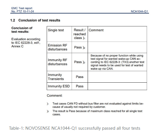
  The IBEE/FTZ-Zwickau certification is carried out according to the IEC 62228-3 standard. Compared with SAE J2962, IEC 62228-3 excludes the effects of peripheral circuits, focuses more on the EMC property of the CAN transceiver itself, and specifies higher performance level requirements. The IEC 62228-3 standard is also extensively adopted by automakers outside of Europe. The IBEE/FTZ-Zwickau certification includes four tests: Emission RF Disturbances, Immunity RF Disturbances, Immunity Transients, and Immunity ESD. NCA1044-Q1 from NOVOSENSE successfully passed all four tests.
NOVOSENSE's NCA1044-Q1 CAN Transceiver Successfully Passes the IBEE/FTZ-Zwickau EMC Certification

  Industry-leading interference immunity

  NCA1044-Q1 features an ingenious circuit design that addresses the issue of output signal errors caused by abnormal high-voltage interference affecting its output circuit. This enhances its EMC performance, helping customers substantially reduce their EMC design complexity, simplify peripheral components, and lower costs.

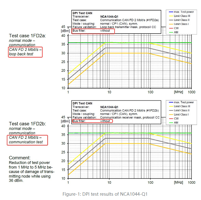
  Furthermore, NCA1044-Q1 boasts industry-leading interference immunity. According to IEC 62228-3, when external RF noise at different frequency bands couples to the CAN bus, a higher pass-through power indicates stronger interference immunity. This means a lower risk of errors in the system.

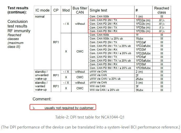
  Even without the use of a common-mode inductor filter on the bus, NCA1044-Q1 from NOVOSENSE can still meet the highest power requirements specified in the standard (as shown in Figure-1 and Table-2). Although this test is typically not required at the application level, NCA1044-Q1 still successfully passed the test. This capability helps users reduce peripheral circuits, lower costs, and enhance system robustness.
NOVOSENSE's NCA1044-Q1 CAN Transceiver Successfully Passes the IBEE/FTZ-Zwickau EMC Certification

  Packages and selection

  NCA1044-Q1 is now in mass production and is available in SOP8 and DFN8 packages. Compliant with the AEC-Q100 Grade 1 requirements, it operates in a wide temperature range from -40°C to 125°C, and provides over-temperature protection. NCA1044-Q1 also supports TXD dominant timeout function and remote wake-up in standby mode. 
NOVOSENSE's NCA1044-Q1 CAN Transceiver Successfully Passes the IBEE/FTZ-Zwickau EMC Certification

("Note: The information presented in this article is gathered from the internet and is provided as a reference for educational purposes. It does not signify the endorsement or standpoint of our website. If you find any content that violates copyright or intellectual property rights, please inform us for prompt removal.")

Online messageinquiry

reading
Adapting to challenging magnetic environments: MT73xx 3D dual-output Hall latches from NOVOSENSE enable precise automotive motor control
  The NOVOSENSE MT73xx series dual-output Hall latches, based on 3D Hall technology, support SS (Speed & Speed) or SD (Speed & Direction) dual-channel outputs and complies with Automotive Grade 0 standards. Ideal for motor control systems such as power windows, liftgates, and sunroofs, this product family enhances the accuracy and stability of speed and position detection, optimizing overall in-vehicle comfort.  In motor control systems, precise detection of speed and direction signals directly influences system response speed and operational stability. Traditional solutions typically rely on a combination of two separate Hall latches, requiring high magnetic ring installation precision. This often leads to issues such as signal phase deviation, poor synchronization, and structural complexity.  Integrates a 3D Hall sensing structure with inherent orthogonal output characteristics, the MT73xx series can simultaneously deliver dual-channel speed signals (SS output) with a 90° phase difference or speed and direction signals (SD output), making it widely suitable for “speed-direction” detection applications. This design reduces dependency on precise positioning of magnetic poles, mitigates dual-channel phase deviation, simplifies system architecture, and improves overall system stability, providing a more flexible and reliable solution for motion control detection.  Compatibility with diverse magnetic ring configurations enabled by VHS technology  To achieve high-precision 3D sensing, the MT73xx series adopts NOVOSENSE’s proprietary VHS (Vertical Hall Sensor) technology. Through combinations of XY, YZ, and XZ axial sensing, any two axes naturally deliver orthogonal outputs, enhancing signal synchronization.  Additionally, the MT73xx series offers excellent compatibility with various magnetic ring configurations – whether axial, radial, or irregularly shaped magnets – maintaining robust duty cycle performance. This allows customers to adapt designs flexibly depending on magnetic ring characteristics and installation environments, further reducing development complexity and tuning costs.  Dual-output design for optimized system integration  Regarding system integration, the MT73xx’s dual-output capability allows it to replace traditional single- or dual-Hall solutions by directly transmitting SS (Speed & Speed) or SD (Speed & Direction) signals to ECU, minimizing the requirements for peripheral redundant position sensors.  This approach not only saves PCB space and simplifies structural layouts, but also enhances solution integration, offering greater design flexibility for innovative applications in motor control and intelligent cockpit systems.
2025-08-13 15:35 reading:376
High-voltage half-bridge driver NSD2622N from NOVOSENSE: A high-reliability, high-integration solution tailored for E-mode GaN
  NOVOSENSE has launched NSD2622N, a high-voltage half-bridge driver IC specifically designed for enhancement-mode GaN (E-mode GaN). This chip integrates positive/negative voltage regulation circuits, supports bootstrap supply, and provides high dv/dt immunity and robust driving capability. It significantly simplifies GaN driver circuit design while enhancing system reliability and reducing overall costs.  Application background  In recent years, gallium nitride high-electron-mobility transistors (GaN HEMTs) are gaining increasingly widespread adoption in high-voltage, high-power applications, such as AI data center power supplies, microinverters, and on-board chargers (OBCs). With significant advantages of high switching frequency and low switching losses, GaN HEMTs enable substantially improved power density in power supply systems, noticeably optimized energy efficiency, and significantly reduced system costs.  However, GaN devices still face challenges in real-world applications. For instance, E-mode GaN devices exhibit low turn-on thresholds. In high-voltage and high-power applications, particularly in hard-switching operation mode, poorly designed driver circuits can lead to false triggering due to crosstalk during high-frequency high-speed switching. Additionally, the complexity of compatible driver circuit designs raises the barrier to GaN device adoption.  To accelerate widespread GaN adoption, leading GaN manufacturers at home and abroad have introduced some power ICs with integrated drivers, especially MOSFET-LIKE GaN power devices in Si-MOSFET-compatible packages, which somewhat reduce GaN driver circuit design complexity. However, driver-integrated GaN solutions have limitations: they struggle to meet customized design requirements and are unsuitable for applications adopting multi-device parallel or bidirectional switching topologies. Therefore, discrete GaN devices with dedicated drivers remain essential for many applications. To address the above-mentioned limitations, NOVOSENSE has developed NSD2622N – a driver IC tailored to E-mode GaN, aiming to deliver high-performance, high-reliability, and cost-competitive driving solutions for high-voltage and high-power GaN applications.  Product features  NSD2622N is a high-voltage half-bridge driver IC specifically designed for E-mode GaN. It integrates a voltage regulation circuit capable of generating a configurable stable positive voltage from 5V to 6.5V to ensure reliable GaN driving, as well as a charge pump circuit that produces a fixed -2.5V negative voltage for reliable GaN turn-off. By integrating both positive and negative voltage regulation circuits, the chip supports high-side output with bootstrap supply.  NSD2622N leverages NOVOSENSE’s proven capacitive isolation technology. Its high-side driver withstands a voltage range of -700V to +700V and a minimum SW dv/dt immunity of 200V/ns. Meanwhile, low propagation delay and tight delay matching between high-side and low-side outputs make it a perfect match for the high-frequency, high-speed switching requirements of GaN devices. Additionally, NSD2622N delivers 2A (source) and -4A (sink) peak drive currents on both high-side and low-side outputs, meeting the requirements of high-speed GaN driving and multi-device parallel configurations. The IC also includes an integrated 5V LDO that can power circuits like digital isolators in applications requiring isolation.  Key specifications of NSD2622N  SW voltage range: -700V to 700V  SW dv/dt immunity: > 200V/ns  Wide supply voltage range: 5V-15V  Adjustable positive output voltage range: 5V-6.5V  Built-in negative output voltage: -2.5V  Peak drive current: 2A (source) / 4A (sink)  Minimum input pulse width (typical): 10ns  Input-to-output propagation delay (typical): 38ns  Pulse width distortion (typical): 5ns  Rise time (1nF load, typical): 6.5ns  Fall time (1nF load, typical): 6.5ns  Built-in dead time (typical): 20ns  Bootstrap supply for high-side output  Integrated 5V LDO for digital isolator supply  Undervoltage lockout (UVLO) and overtemperature protection  Operating temperature range: -40°C to +125°CFunctional block diagram of NSD2622N  Eliminating false triggering risks and providing more stable drive voltage  Compared to conventional Si MOSFET driver solutions, the key challenge in E-mode GaN driver circuit design lies in providing appropriate, stable and reliable positive/negative bias voltages. This is because that E-mode GaN typically requires a 5V-6V turn-on voltage, while its threshold voltage is as low as 1V, or even lower at high temperatures, necessitating negative turn-off voltage to prevent false triggering. To address this challenge, two common drive solutions are used for E-mode GaN: resistive-capacitive (RC) voltage division drive and direct drive.  1. RC voltage division drive  This approach utilizes standard Si MOSFET driver ICs. As shown in the diagram, during turn-on, the parallel combination of Cc and Ra is connected with Rb in series, dividing the driver supply voltage (e.g., 10V) to provide a 6V gate drive voltage for the GaN device, with Dz1 clamping the positive voltage. During turn-off, Cc discharges to provide negative turn-off voltage for the GaN device, with Dz2 clamping the negative voltage.RC voltage division drive solution  Although the RC voltage division circuit does not require sophisticated driver ICs, it introduces additional parasitic inductance due to a large number of components involved, which can impact GaN’s switching performance at high frequencies. Moreover, since the negative turn-off voltage relies on discharge from capacitor Cc, the negative turn-off voltage proves unreliable.  As shown in the half-bridge demo board test waveforms, during the startup phase (T1 in the waveform), the absence of initial charge on Cc results in failure to establish negative voltage and thus zero-voltage turn-off; during the negative turn-off period following the driver’s signal transmission (T2), the negative voltage amplitude fluctuates with capacitor discharge; and during the prolonged turn-off period (T3), the capacitor cannot sustain negative voltage, eventually discharging to zero. Consequently, RC voltage division circuits are generally limited to medium/low power applications with relatively lower reliability requirements, and are proved unsuitable for high-power systems.Waveform of E-mode GaN using RC voltage division drive circuit(CH2: Drive supply voltage; CH3: GaN gate-source voltage)  2. Direct drive  The direct drive solution requires selecting a driver IC with an appropriate undervoltage-lockout (UVLO) threshold, for example, NSI6602VD, which is specifically designed for E-mode GaN with a 4V UVLO threshold. When paired with an external positive/negative voltage regulation circuit, it can directly drive E-mode GaN devices. Below is a typical application circuit.NSI6602VD driver circuitPositive and negative voltage regulation circuits  This direct drive solution can provide reliable negative turn-off voltage for GaN under all operating conditions, when the auxiliary power supply is functioning normally. As a result, this approach is widely adopted in various high-voltage, high-power GaN applications.  The next-generation GaN driver NSD2622N from NOVOSENSE, integrates the positive/negative voltage regulation circuits directly into the chip. As shown in the half-bridge demo board test waveforms below, NSD2622N maintains consistent negative turn-off voltage amplitude and duration regardless of operating conditions. Specifically, during startup (T1 in the waveform), the negative voltage is established even before the driver sends signals; during GaN turn-off (T2), the negative voltage remains stable in amplitude; during extended periods without driver signals (T3), the negative voltage continues to stay reliably stable.Waveforms of E-mode GaN using NSD2622N driver circuit(CH2: Low-side GaN Vds, CH3: Low-side GaN Vgs)  Simplified circuit design and reduced system costs  NSD2622N can provide stable and reliable direct drive for GaN devices. More importantly, by integrating positive/negative voltage regulators, it significantly reduces external component count. By adopting the bootstrap supply architecture, NSD2622N greatly simplifies driver power circuit design and lowers overall system costs.  Taking a 3kW power supply unit (PSU) as an example, assuming both phases of the interleaved TTP PFC and full-bridge LLC use GaN devices, a complexity comparison between two direct-drive solutions is given below:  When using the NSI6602VD driver solution, each half-bridge high-side driver requires an independent isolated power supply in conjunction with corresponding isolation and positive/negative voltage regulation circuits. This means complex auxiliary power supply design for isolation. Given the high power quality requirements of GaN driving and the fact that the main power paths of the PFC and LLC stages are typically placed on separate boards, a two-stage auxiliary power architecture is often necessary. In this configuration, the first stage typically employs a device with wide input voltage range like flyback converter, to generate regulated voltage rails. The second stage may use an open-loop full-bridge topology to provide isolated power and further regulate the power to generate the required positive and negative supply voltages for NSI6602VD. Below is a typical power architecture for such a driver solution.Typical power architecture for NSI6602VD driver solution  The NSD2622N driver solution significantly simplifies auxiliary power design through its bootstrap supply capability. Below is a typical power architecture for this approach.Typical power architecture for NSD2622N driver solution  A detailed comparison of bill-of-materials (BOM) for driver and power supply circuits between the above-mentioned two GaN direct-drive solutions is provided in the table below. It can be seen that the NSD2622N solution utilizing bootstrap supply, dramatically reduces total component count compared to the NSI6602VD’s isolated power supply approach, resulting in substantially lower system costs. Even in applications requiring isolated power supply, NSD2622N maintains its competitive edge - its integrated positive/negative voltage regulators enable a more simplified peripheral circuit relative to the NSI6602VD solution, leading to fewer components and lower system costs.BOM comparison between two GaN direct drive solutions  Versatile GaN compatibility and flexible drive voltage adjustment  The E-mode GaN driver IC NSD2622N from NOVOSENSE delivers not only superior performance but also broad compatibility across various GaN devices from different brands, of different types (including both voltage-mode and current-mode), and at different voltage ratings. For instance, the output voltage of NSD2622N can be set between 5V to 6.5V by adjusting feedback resistors. This enables selection of the most appropriate driving voltage for any GaN device by simply adjusting the feedback resistors to match specific GaN characteristics, allowing GaN devices from different brands to operate at their individual peak performance points.  In addition, NSD2622N features a minimum dv/dt immunity of 200V/ns on the switching node (SW), enhancing the upper limit of GaN switching speed. The adoption of a more compact QFN package and the design of independent turn-on and turn-off output pins further reduce the driver loop parasitic inductance. The over-temperature protection ensures safer GaN applications.  NOVOSENSE also offers single-channel GaN driver IC NSD2012N. Featuring 3mm*3mm QFN package and adjustable negative voltage capability, it can meet more personalized application requirements.
2025-08-07 14:08 reading:453
NOVOSENSE Launches High-Performance 2-Wire Hall Switch MT72xx Series: Compact Design with System-Level Reliability
  NOVOSENSE Microelectronics ("NOVOSENSE") has launched the MT72xx series, 2-wire current output Hall switches. The switches feature superior EMC performance, multiple sensing polarity options, and highly integrated design, achieving ASIL-A functional safety certification and full compliance with AEC-Q100 Grade 0 standards. Designed for long-wiring scenarios in vehicle body electronics and domain controller systems, the MT72xx series provides optimized solutions for seatbelt buckle detection, window lift motor control, and other automotive applications.  Addressing Long Wiring Harness Challenges in Automotive  With rapid advancement of automotive intelligence and electrification, increasingly complex vehicle body functions and highly integrated domain controllers have significantly extended wiring harnesses between sensors and control units. This introduces critical challenges including elevated signal interference risks, increased costs, and compromised system reliability.  NOVOSENSE's MT72xx series delivers robust signal integrity while effectively reducing wiring complexity and lowering harness costs. Designed for long-wiring scenarios such as door lock detection, anti-pinch window control, power tailgate position sensing, seat adjustment, and seatbelt buckle detection, these devices provide stable current output with superior anti-interference capabilities, maintaining signal reliability even in extended wiring conditions.  High Integration & Robustness for Automotive-Grade Standards  Engineered for harsh automotive environments with strong EMI interference, the MT72xx series integrates a 100nF(only TO92S package)capacitor to enhance EMC/ESD performance, simplify peripheral configuration, and optimize BOM space, enabling flexible system architecture design. Compliant with AEC-Q100 Grade 0, the devices ensure long-term stability under extreme high-temperature conditions.  Featuring multiple sensing polarity options (unipolar, omnipolar, latch) and adjustable sensitivity thresholds, the MT72xx series offers design flexibility to accommodate diverse magnet solutions and vehicle architectures, streamlining development and debugging processes.  Comprehensive Resources to Accelerate Time-to-Market  To expedite customer development, NOVOSENSEN provides dedicated MT72xx demo boards and magnetic simulation services. These resources enable rapid device validation, magnet solution matching, and cost-effective debugging, significantly shortening product deployment cycles.
2025-07-14 14:25 reading:534
NOVOSENSE introduces NSDA6934-Q1: Automotive-grade Class D audio amplifier with digital input
  NOVOSENSE recently announced the launch of the NSDA6934-Q1, a digital-input automotive-grade Class D audio amplifier designed for vehicle audio systems. Featuring four-channel audio output with up to 75W per channel, it supports low-latency mode and sampling rates up to 192kHz. The amplifier offers flexible switching frequencies, multiple modulation options, and comprehensive protection features, making it highly adaptable to various automotive audio system designs.  Class D amplifiers: Driving the evolution of automotive audio  As automotive electronics continue to advance, Class D amplifiers have emerged as the preferred choice for vehicle audio systems due to their high efficiency, low heat dissipation, and compact form factor. These amplifiers not only meet modern vehicles’ stringent energy efficiency demands but also enhance audio quality and power output within limited space, playing a key role in the evolution of automotive audio technology.  Optimized Low-Latency Mode: Reducing Path Delay by Over 70%  In automotive audio systems, amplifiers boost signals from the DSP (Digital Signal Processor) before transmitting them to the speakers. Traditional amplifiers can contribute to over 30% of total signal transmission latency, impacting system performance.  The NSDA6934-Q1 features a unique low-latency mode that reduces transmission path delay by more than 70%, granting the DSP additional time for signal processing. This reduces DSP resource demands and enhances the effectiveness of RNC (Road Noise Cancellation). Additionally, the amplifier supports up to 192kHz sampling rates, delivering high-resolution audio with enhanced clarity and detail for an immersive in-car listening experience.  Flexible Configurations to Suit Various Designs  The NSDA6934-Q1 provides a wide range of switching frequencies and modulation options, allowing system engineers to optimize efficiency and size.  Adjustable Switching Frequency (384kHz – 2.1MHz)  At 384kHz, the amplifier achieves up to 93% efficiency, ideal for applications prioritizing power savings, though it requires a 10μH inductor for operation.  At 2.1MHz, the amplifier supports a compact 3.3μH inductor, making it suitable for space-constrained smart cockpit integration.  Selectable Modulation Modes (BD Mode & 1SPW Mode)  BD Mode (50% duty cycle) ensures superior linearity at high power levels, making it ideal for high-output applications.  1SPW Mode (20% duty cycle) reduces conduction losses, improving efficiency in low-power scenarios  Additionally, the NSDA6934-Q1 supports TDM16 data format, ensuring seamless integration with mainstream audio interfaces. With eight selectable I2C addresses, it prevents communication conflicts among peripheral devices. It also features integrated PVDD voltage monitoring, eliminating the need for external resistor dividers and simplifying system wiring and debugging.  Enhanced EMC Performance & Comprehensive Protection  The NSDA6934-Q1 incorporates multiple EMC optimization techniques, including slew rate control, phase control, and three spread-spectrum modes (triangular wave, random spread, hybrid spread), helping customers pass system-level EMC tests efficiently.For system reliability, the amplifier integrates multiple intelligent protection and diagnostic functions, including:  • I2C watchdog for real-time bus monitoring.  • Thermal protection, which automatically reduces gain under high-temperature conditions.  • AC/DC diagnostics for real-time power supply monitoring.  • Comprehensive protection suite, including temperature alarms, over-temperature shutdown, undervoltage, overvoltage, and overcurrent protection, ensuring robust system stability.
2025-04-24 17:19 reading:682
  • Week of hot material
  • Material in short supply seckilling
model brand Quote
RB751G-40T2R ROHM Semiconductor
BD71847AMWV-E2 ROHM Semiconductor
TL431ACLPR Texas Instruments
CDZVT2R20B ROHM Semiconductor
MC33074DR2G onsemi
model brand To snap up
IPZ40N04S5L4R8ATMA1 Infineon Technologies
BP3621 ROHM Semiconductor
ESR03EZPJ151 ROHM Semiconductor
STM32F429IGT6 STMicroelectronics
TPS63050YFFR Texas Instruments
BU33JA2MNVX-CTL ROHM Semiconductor
Hot labels
ROHM
IC
Averlogic
Intel
Samsung
IoT
AI
Sensor
Chip
About us

Qr code of ameya360 official account

Identify TWO-DIMENSIONAL code, you can pay attention to

AMEYA360 weixin Service Account AMEYA360 weixin Service Account
AMEYA360 mall (www.ameya360.com) was launched in 2011. Now there are more than 3,500 high-quality suppliers, including 6 million product model data, and more than 1 million component stocks for purchase. Products cover MCU+ memory + power chip +IGBT+MOS tube + op amp + RF Bluetooth + sensor + resistor capacitance inductor + connector and other fields. main business of platform covers spot sales of electronic components, BOM distribution and product supporting materials, providing one-stop purchasing and sales services for our customers.

Please enter the verification code in the image below:

verification code